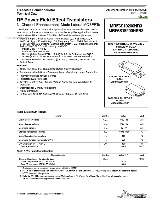
Datasheet4U Logo Datasheet4U.com

MRF6S19200HSR3 - RF Power Transistors

Download the MRF6S19200HSR3 datasheet PDF. This datasheet also covers the MRF6S19200HR3 variant, as both devices belong to the same rf power transistors family and are provided as variant models within a single manufacturer datasheet.

General Description

Short Ferrite Bead 10 μF, 50 V Electrolytic Capacitor 0.1 μF, 100 V Capacitors 33 pF Chip Capacitors 10 pF Chip Capacitors 10 μF, 50 V Capacitors 22 μF, 35 V Tantalum Capacitors 22 μF, 50 V Electrolytic Capacitors 1000 Ω, 1/4 W Chip Resistor 10 Ω, 1/4 W Chip Resistor Part Number 2743019447 EMVY500AD

Key Features

  • 100% PAR Tested for Guaranteed Output Power Capability.
  • Characterized with Series Equivalent Large - Signal Impedance Parameters.
  • Internally Matched for Ease of Use.
  • Integrated ESD Protection.
  • Greater Negative Gate - Source Voltage Range for Improved Class C Operation.
  • Optimized for Doherty.

📥 Download Datasheet

Note: The manufacturer provides a single datasheet file (MRF6S19200HR3_FreescaleSemiconductor.pdf) that lists specifications for multiple related part numbers.

Full PDF Text Transcription (Reference)

The following content is an automatically extracted verbatim text from the original manufacturer datasheet and is provided for reference purposes only.

View original datasheet text
Freescale Semiconductor Technical Data Document Number: MRF6S19200H Rev. 0, 3/2008 RF Power Field Effect Transistors N - Channel Enhancement - Mode Lateral MOSFETs Designed for CDMA base station applications with frequencies from 1930 to 1990 MHz. Suitable for CDMA and multicarrier amplifier applications. To be used in Class AB and Class C for PCN - PCS/cellular radio applications. www.datasheet4u.com • Typical Single - Carrier W - CDMA Performance: VDD = 28 Volts, IDQ = 1600 mA, Pout = 56 Watts Avg., Full Frequency Band, 3GPP Test Model 1, 64 DPCH with 50% Clipping, Channel Bandwidth = 3.84 MHz, Input Signal PAR = 7.5 dB @ 0.01% Probability on CCDF. Power Gain — 17.9 dB Drain Efficiency — 29.5% Device Output Signal PAR — 5.9 dB @ 0.