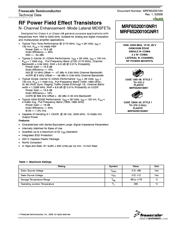
Datasheet4U Logo Datasheet4U.com

MRF6S20010NR1 - RF Power Field Effect Transistors

Description

100 nF Chip Capacitor (1206) 4.7 pF 600B Chip Capacitors 9.1 pF 600B Chip Capacitors 10 μF, 50 V Chip Capacitors 10 μF, 35 V Tantalum Chip Capacitor 1 kΩ Chip Resistor (1206) 10 kΩ Chip Resistor (1206) 10 Ω Chip Resistor (1206) Part Number CDR33BX104AKWS 600B4R7CW 600B9R1CW GRM55DR61H106KA88B T490D1

Features

  • Characterized with Series Equivalent Large - Signal Impedance Parameters.
  • Internally Matched for Ease of Use.
  • Qualified Up to a Maximum of 32 VDD Operation.
  • Integrated ESD Protection.
  • 200°C Capable Plastic Package.
  • RoHS Compliant.
  • In Tape and Reel. R1 Suffix = 500 Units per 24 mm, 13 inch Reel. MRF6S20010NR1 MRF6S20010GNR1 1600 - 2200 MHz, 10 W, 28 V GSM/GSM EDGE SINGLE N - CDMA 2 x W - CDMA.

📥 Download Datasheet

Datasheet preview – MRF6S20010NR1

Datasheet Details

Part number MRF6S20010NR1
Manufacturer Freescale Semiconductor
File Size 627.46 KB
Description RF Power Field Effect Transistors
Datasheet download datasheet MRF6S20010NR1 Datasheet
Additional preview pages of the MRF6S20010NR1 datasheet.
Other Datasheets by Freescale Semiconductor

Full PDF Text Transcription

Click to expand full text
www.DataSheet4U.com Freescale Semiconductor Technical Data Document Number: MRF6S20010N Rev. 1, 5/2006 RF Power Field Effect Transistors N - Channel Enhancement - Mode Lateral MOSFETs Designed for Class A or Class AB general purpose applications with frequencies from 1600 to 2200 MHz. Suitable for analog and digital modulation and multipurpose amplifier applications. • Typical Two - Tone Performance @ 2170 MHz: VDD = 28 Volts, IDQ = 130 mA, Pout = 10 Watts PEP Power Gain — 15.5 dB Drain Efficiency — 36% IMD — - 34 dBc • Typical 2 - Carrier W - CDMA Performance: VDD = 28 Volts, IDQ = 130 mA, Pout = 1 Watt Avg., Full Frequency Band (2130 - 2170 MHz), Channel Bandwidth = 3.84 MHz. PAR = 8.5 dB @ 0.01% Probability Power Gain — 15.
Published: |