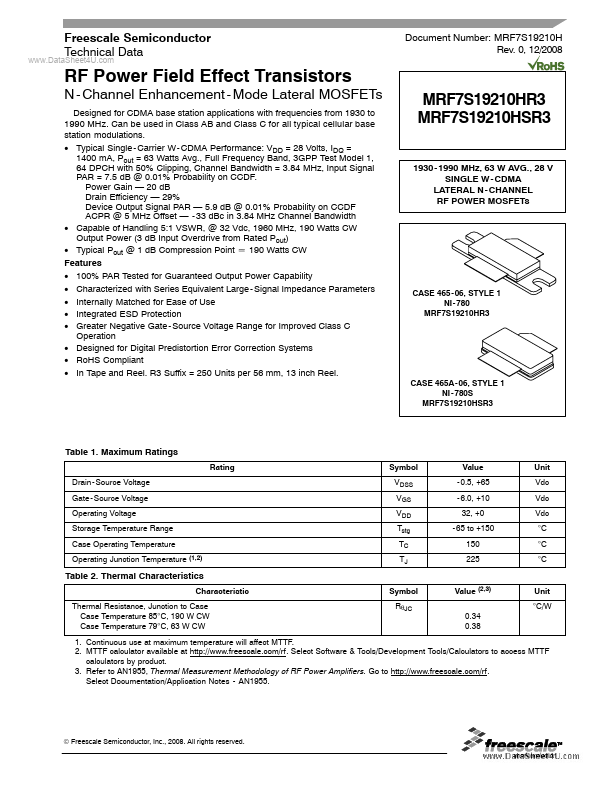
Datasheet4U Logo Datasheet4U.com

MRF7S19210HR3 - RF Power Field Effect Transistors

Description

10 μF, 50 V Chip Capacitors 100 nF Chip Capacitors 8.2 pF Chip Capacitors 0.2 pF Chip Capacitor 1.8 pF Chip Capacitor 0.4 pF Chip Capacitor 0.5 pF Chip Capacitors 470 μF Electrolytic Capacitors 10 kΩ, 1/4 W Chip Resistors 10 Ω, 1/4 W Chip Resistor Part Number C5750X5R1H106M 12065C104KAT2A ATC100B8R2

Features

  • 100% PAR Tested for Guaranteed Output Power Capability.
  • Characterized with Series Equivalent Large - Signal Impedance Parameters.
  • Internally Matched for Ease of Use.
  • Integrated ESD Protection.
  • Greater Negative Gate - Source Voltage Range for Improved Class C Operation.
  • Designed for Digital Predistortion Error Correction Systems.
  • RoHS Compliant.
  • In Tape and Reel. R3 Suffix = 250 Units per 56 mm, 13 inch Reel. MRF7S19210HR3.

📥 Download Datasheet

Datasheet preview – MRF7S19210HR3

Datasheet Details

Part number MRF7S19210HR3
Manufacturer Freescale Semiconductor
File Size 546.69 KB
Description RF Power Field Effect Transistors
Datasheet download datasheet MRF7S19210HR3 Datasheet
Additional preview pages of the MRF7S19210HR3 datasheet.
Other Datasheets by Freescale Semiconductor

Full PDF Text Transcription

Click to expand full text
www.DataSheet4U.com Freescale Semiconductor Technical Data Document Number: MRF7S19210H Rev. 0, 12/2008 RF Power Field Effect Transistors N - Channel Enhancement - Mode Lateral MOSFETs Designed for CDMA base station applications with frequencies from 1930 to 1990 MHz. Can be used in Class AB and Class C for all typical cellular base station modulations. • Typical Single - Carrier W - CDMA Performance: VDD = 28 Volts, IDQ = 1400 mA, Pout = 63 Watts Avg., Full Frequency Band, 3GPP Test Model 1, 64 DPCH with 50% Clipping, Channel Bandwidth = 3.84 MHz, Input Signal PAR = 7.5 dB @ 0.01% Probability on CCDF. Power Gain — 20 dB Drain Efficiency — 29% Device Output Signal PAR — 5.9 dB @ 0.01% Probability on CCDF ACPR @ 5 MHz Offset — - 33 dBc in 3.
Published: |