MRF8S9200NR3
MRF8S9200NR3 is RF Power Field Effect Transistor manufactured by Freescale Semiconductor.
Features
- 100% PAR Tested for Guaranteed Output Power Capability
- Characterized with Series Equivalent Large
- Signal Impedance Parameters and mon Source S
- Parameters
- Internally Matched for Ease of Use
- Integrated ESD Protection
- Greater Negative Gate
- Source Voltage Range for Improved Class C Operation
- 225°C Capable Plastic Package
- Designed for Digital Predistortion Error Correction Systems
- Optimized for Doherty Applications
- Ro HS pliant
- In Tape and Reel. R3 Suffix = 250 Units per 32 mm, 13 inch Reel.
.. Table 1. Maximum Ratings Rating Drain
- Source Voltage Gate
- Source Voltage Operating Voltage Storage Temperature Range Case Operating Temperature Operating Junction Temperature (1,2) Symbol VDSS VGS VDD Tstg TC TJ
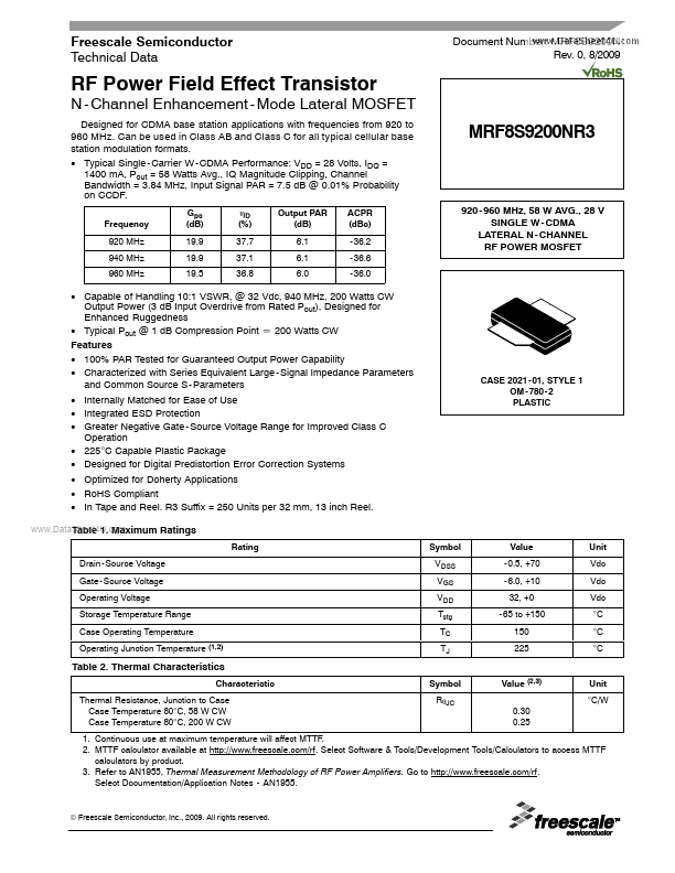
CASE 2021
- 01, STYLE 1 OM
- 780
- 2 PLASTIC
Value
- 0.5, +70
- 6.0, +10 32, +0
- 65 to +150 150 225
Unit Vdc Vdc Vdc °C °C °C
Table 2. Thermal Characteristics
Characteristic Thermal Resistance, Junction to Case Case Temperature 80°C, 58 W CW Case Temperature 80°C, 200 W CW Symbol RθJC Value (2,3) 0.30 0.25 Unit °C/W
1. Continuous use at maximum temperature will affect MTTF. 2. MTTF calculator available at http://.freescale./rf. Select Software & Tools/Development Tools/Calculators to access MTTF calculators by product. 3. Refer to AN1955, Thermal Measurement Methodology of RF Power Amplifiers. Go to http://.freescale./rf. Select Documentation/Application Notes
- AN1955.
© Freescale Semiconductor, Inc., 2009. All rights reserved.
MRF8S9200NR3 1
RF Device Data Freescale Semiconductor
Table 3. ESD Protection Characteristics
Test Methodology Human Body Model (per JESD22
- A114) Machine Model (per EIA/JESD22
- A115) Charge Device Model (per JESD22
- C101) Class 1C (Minimum) A (Minimum) IV (Minimum)
Table 4. Moisture Sensitivity Level
Test Methodology Per...