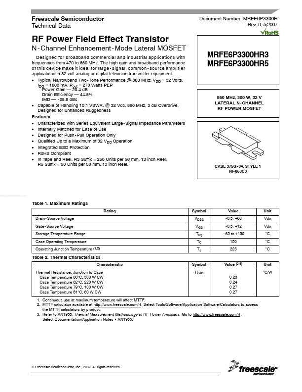
MRFE6P3300HR3
MRFE6P3300HR3 is RF Power Field Effect Transistor manufactured by Freescale Semiconductor.
Features
- Characterized with Series Equivalent Large
- Signal Impedance Parameters
- Internally Matched for Ease of Use
- Designed for Push
- Pull Operation Only
- Qualified Up to a Maximum of 32 VDD Operation
- Integrated ESD Protection
- Ro HS pliant
- In Tape and Reel. R3 Suffix = 250 Units per 56 mm, 13 inch Reel. R5 Suffix = 50 Units per 56 mm, 13 inch Reel.
MRFE6P3300HR3 MRFE6P3300HR5
860 MHz, 300 W, 32 V LATERAL N
- CHANNEL RF POWER MOSFET
CASE 375G
- 04, STYLE 1 NI
- 860C3
..
Table 1. Maximum Ratings
Rating Drain
- Source Voltage Gate
- Source Voltage Storage Temperature Range Case Operating Temperature Operating Junction Temperature (1,2) Symbol VDSS VGS Tstg TC TJ Value
- 0.5, +66
- 0.5, +12
- 65 to +150 150 225 Unit Vdc Vdc °C °C °C
Table 2. Thermal Characteristics
Characteristic Thermal Resistance, Junction to Case Case Temperature 80°C, 300 W CW Case Temperature 82°C, 220 W CW Case Temperature 79°C, 100 W CW Case Temperature 81°C, 60 W CW Symbol RθJC Value (2,3) 0.23 0.24 0.27 0.27 Unit °C/W
1. Continuous use at maximum temperature will affect MTTF. 2. MTTF calculator available at http://.freescale./rf. Select Tools/Software/Application Software/Calculators to access the MTTF calculators by product. 3. Refer to AN1955, Thermal Measurement Methodology of RF Power Amplifiers. Go to http://.freescale./rf. Select Documentation/Application Notes
- AN1955.
© Freescale Semiconductor, Inc., 2007. All rights reserved.
MRFE6P3300HR3 MRFE6P3300HR5 1
RF Device Data Freescale Semiconductor
Table 3. ESD Protection Characteristics
Test Methodology Human Body Model (per JESD22
- A114) Machine Model (per EIA/JESD22
- A115) Charge Device Model (per JESD22
- C101) Class 3B (Minimum) C (Minimum) IV (Minimum)
Table 4. Electrical Characteristics (TC = 25°C unless otherwise noted)
Characteristic Off Characteristics
(1)
Symbol IDSS IDSS...