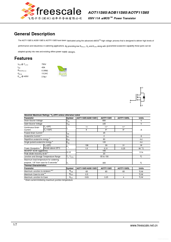
AOT11S65
Overview
The AOT11S65 & AOB11S65 & AOTF11S65 have been fabricated using the advanced αMOSTM high voltage process that is designed to deliver high levels of performance and robustness in switching applications. By providing low RDS(on), Qg and EOSS along with guaranteed avalanche capability these parts can be adopted quickly into new and existing offline power supply designs.
- G S C unless otherwise noted Absolute Maximum Ratings TA=25° Symbol AOT11S65/AOB11S65 Parameter VDS Drain-Source Voltage Gate-Source Voltage Continuous Drain Current Pulsed Drain Current Avalanche Current C Repetitive avalanche energy C Single pulsed avalanche energy G C TC=25° Power Dissipation B Derate above 25oC MOSFET dv/dt ruggedness H Peak diode recovery dv/dt Junction and Storage Temperature Range Maximum lead temperature for soldering purpose, 1/8" from case for 5 seconds J Thermal Characteristics Parameter Maximum Junction-to-Ambient A,D C