Datasheet4U Logo Datasheet4U.com

MRFE6S8046GNR1 Datasheet Rf Power Field Effect Transistors

Manufacturer: Freescale Semiconductor (now NXP Semiconductors)

Overview: 
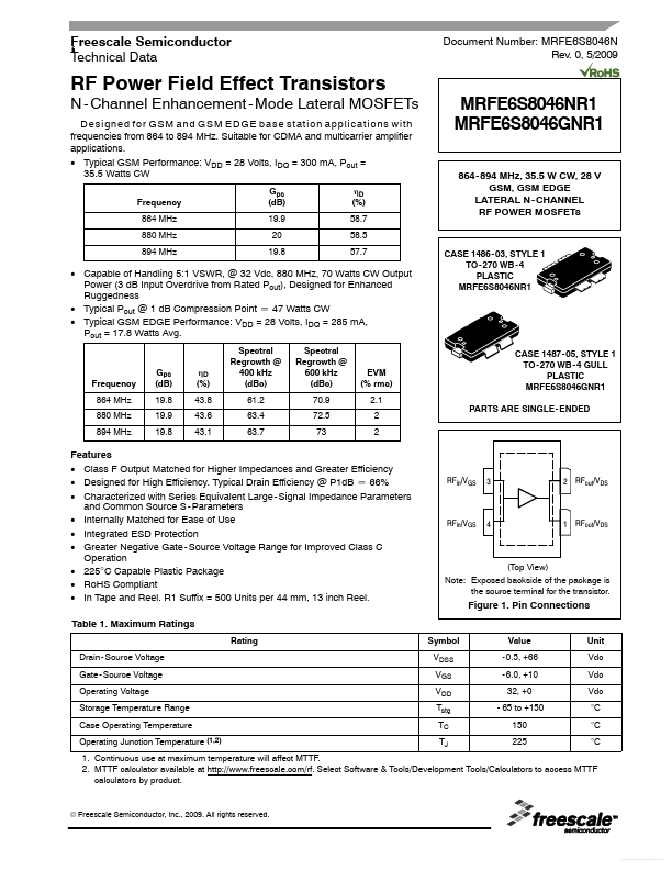
Freescale Semiconductor ‘ Technical Data Document Number: MRFE6S8046N Rev. 0, 5/2009 RF Power Field Effect Transistors N - Channel Enhancement - Mode Lateral MOSFETs Designed for GSM and GSM EDGE base station applications with frequencies from 864 to 894 MHz. Suitable for CDMA and multicarrier amplifier applications. • Typical GSM Performance: VDD = 28 Volts, IDQ = 300 mA, Pout = 35.5 Watts CW Frequency 864 MHz 880 MHz 894 MHz Gps (dB) 19.9 20 19.8 hD (%) 58.7 58.5 57.7 MRFE6S8046NR1 MRFE6S8046GNR1 864 - 894 MHz, 35.5 W CW, 28 V GSM, GSM EDGE LATERAL N - CHANNEL RF POWER MOSFETs • Capable of Handling 5:1 VSWR, @ 32 Vdc, 880 MHz, 70 Watts CW Output Power (3 dB Input Overdrive from Rated Pout), Designed for Enhanced Ruggedness • Typical Pout @ 1 dB pression Point ] 47 Watts CW • Typical GSM EDGE Performance: VDD = 28 Volts, IDQ = 285 mA, Pout = 17.8 Watts Avg. Spectral Regrowth @ 400 kHz (dBc) 61.2 63.4 63.7 Spectral Regrowth @ 600 kHz (dBc) 70.9 72.5 73 CASE 1486 - 03, STYLE 1 TO - 270 WB - 4 PLASTIC MRFE6S8046NR1 Frequency 864 MHz 880 MHz 894 MHz Gps (dB) 19.8 19.9 19.8 hD (%) 43.8 43.6 43.1 EVM (% rms) 2.

This datasheet includes multiple variants, all published together in a single manufacturer document.

Key Features

  • Class F Output Matched for Higher Impedances and Greater Efficiency.
  • Designed for High Efficiency. Typical Drain Efficiency @ P1dB ] 66%.
  • Characterized with Series Equivalent Large - Signal Impedance Parameters and Common Source S - Parameters.
  • Internally Matched for Ease of Use.
  • Integrated ESD Protection.
  • Greater Negative Gate - Source Voltage Range for Improved Class C Operation.
  • 225°C Capable Plastic Package.
  • RoHS Compli.

MRFE6S8046GNR1 Distributor