2SK3589-01
Features
High speed switching Low on-resistance No secondary breadown Low driving power Avalanche-proof
N-CHANNEL SILICON POWER MOSFET FUJI POWER MOS FET
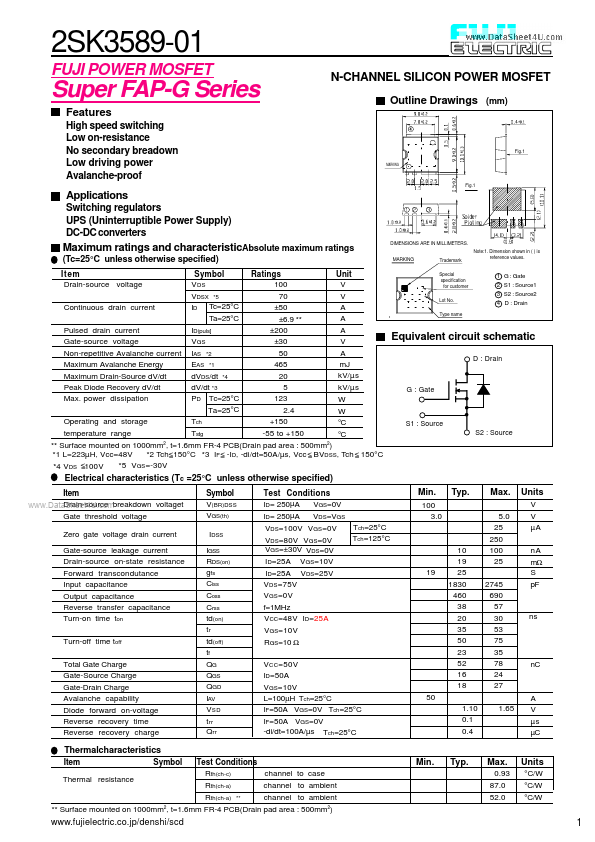
Outline Drawings (mm) O Š }- @- ¡`Œ
OUT VIEW
Fig.1 o ‚Q Ž}‹- î- Æ-
MARKING
- Ž ¦ “ à
- e
Fig.1
Applications
Switching regulators UPS (Uninterruptible Power Supply) DC-DC converters o ‚ }‹- Žî-
Maximum ratings and characteristic Absolute maximum ratings
(Tc=25°C unless otherwise specified)
Item Drain-source voltage Continuous drain current Pulsed drain current Gate-source voltage Non-repetitive Avalanche current Maximum Avalanche Energy Maximum Drain-Source d V/dt Peak Diode Recovery d V/dt Max. power dissipation Operating and storage temperature range Symbol V DS VDSX
- 5 ID Tc=25°C Ta=25°C ID(puls] VGS IAS
- 2 EAS
- 1 d VDS/dt
- 4 d V/dt
- 3 PD Tc=25°C Ta=25°C Tch Tstg Ratings 100 70 ±50 ±6.9
- - ±200 ±30 50 465 20 5 123 2.4 +150 Unit V V A A A V A m J k V/µs k V/µs W W °C °C
DIMENSIONS ARE IN MILLIMETERS. MARKING Trademark Note:1....