Datasheet Summary
.DataSheet.co.kr http://.fujielectric./products/semiconductor/
Super J-MOS series
Features
Low on-state resistance Low switching loss easy to use (more controllabe switching dV/dt by Rg)
FUJI POWER MOSFET
N-Channel enhancement mode power MOSFET
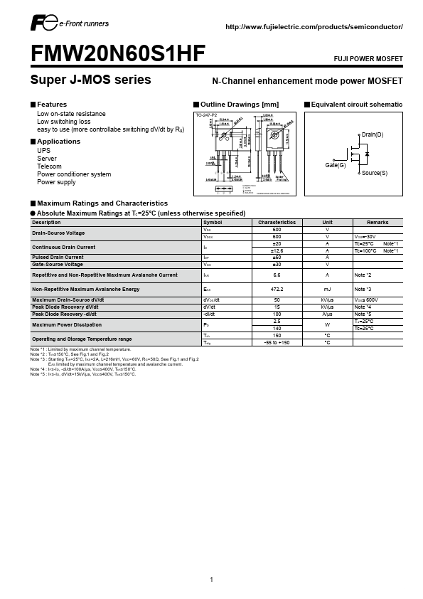
Outline Drawings [mm]
TO-247-P2
Equivalent circuit schematic
Applications
UPS Server Tele Power conditioner system Power supply
Gate(G)
Drain(D)
Source(S)
CONNECTION ① GATE ② DRAIN ③ SOURCE DIMENSIONS ARE IN MILLIMETERS.
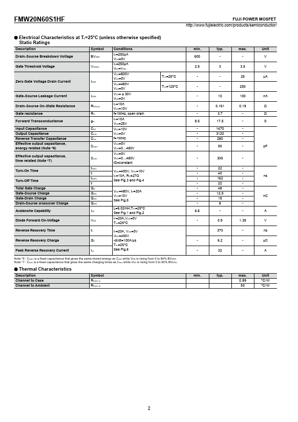
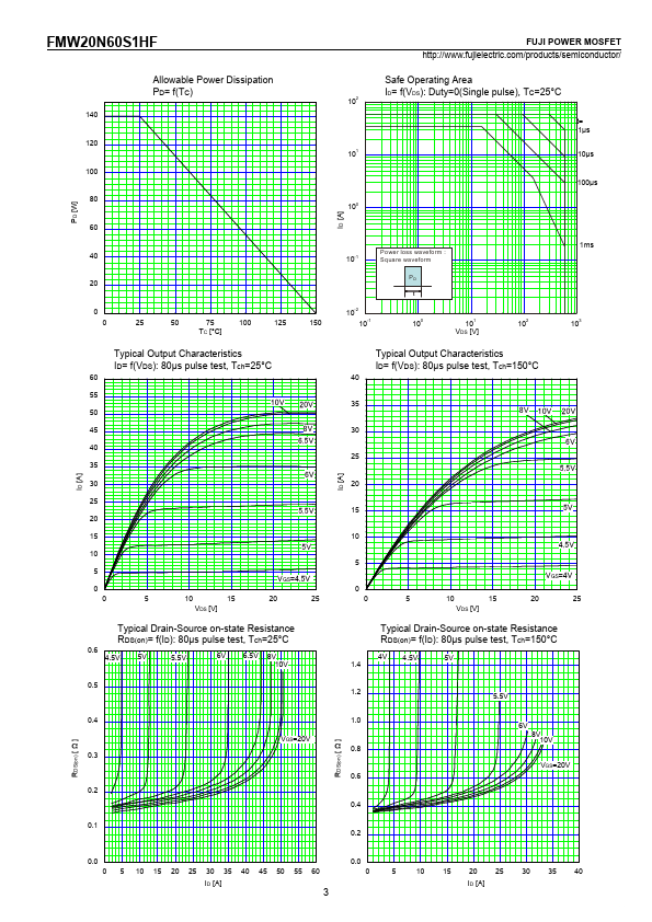
Maximum Ratings and Characteristics...