Fuji Electric 7MBP75TEA060
IGBT
| Part No. | 7MBP75TEA060 |
|---|---|
| Datasheet | 7MBP75TEA060 Download |
| Manufacturer |  Fuji Electric |
| Description | IGBT |
| Buy | Stock & Price |
DESCRIPTION
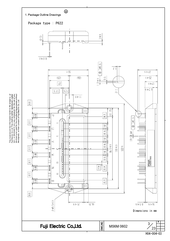
Positive input supply voltage. Output (U). Output (V). Output (W). Negative input supply voltage. Collector terminal of Brake IGBT. Control circuit № ① ② ③ ④ SymbolDESCRIPTION
GNDU High side ground (U). ALMU Alarm signal output (U). VinU Logic input for IGBT gate drive (U). VccU High side supply voltage (U). ⑤ GNDV High side ground (V). ⑥ ALMV Alarm signal output (V). ⑦ VinV Logic input for IGBT gate drive (V). ⑧ VccV High side supply voltage (V). ⑨ GNDW High side ground (W). ⑩ ALMW Alarm signal output (W). ⑪ VinW Logic input for IGBT gate drive (W). ⑫ VccW High side supply voltage (W). ⑬ GND Low side ground. ⑭ Vcc Low side supply voltage. ⑮ VinDB Logic input for Brake IGBT gate drive. ⑯ VinX Logic input for IGBT gate drive (X). ⑰ VinY Logic input for IGBT gate drive (Y). ⑱ VinZ Logic input for IGBT gate drive (Z). ⑲ ALM Low side alarm signal output. MS6M 0602 a 4 23 H04-004-03 3. Block Diagram a VccU ④ VinU ③ ALMU ② GNDU ① RALM 1.5k VccV ⑧ VinV ⑦ ALMV ⑥ GNDV ⑤ RALM 1.5k V...