FMH06N90E
FMH06N90E is N-CHANNEL SILICON POWER MOSFET manufactured by Fuji Electric.
Features
Maintains both low power loss and low noise Lower RDS(on) characteristic More controllable switching dv/dt by gate resistance Smaller VGS ringing waveform during switching Narrow band of the gate threshold voltage (4.0±0.5V) High avalanche durability
FUJI POWER MOSFET
N-CHANNEL SILICON POWER MOSFET
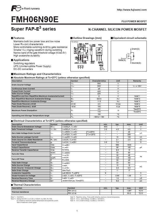
Outline Drawings [mm]
TO-3P(Q)
Equivalent circuit schematic
Drain(D)
Applications
Switching regulators UPS (Uninterruptible Power Supply) DC-DC converters
GATE DRAIN SOURCE JEDEC:TO-3P
Gate(G) Source(S)
Maximum Ratings and Characteristics
Absolute Maximum Ratings at Tc=25°C (unless otherwise specified)
Description
Drain-Source Voltage Continuous Drain Current Pulsed Drain Current Gate-Source Voltage Repetitive and Non-Repetitive Maximum Avalanche Current Non-Repetitive Maximum Avalanche Energy Repetitive Maximum Avalanche Energy Peak Diode Recovery d V/dt Peak Diode Recovery -di/dt Maximum Power Dissipation Operating and Storage Temperature range Symbol VDS VDSX ID I DP VGS IAR E AS E AR d V/dt -di/dt PD Tch Tstg Characteristics 900 900 ±6 ±24 ±30 6 323.6 11.5 2.0 100 2.5 115 150 -55 to + 150 Unit V V A A V A m J m J k V/µs A/µs W °C °C Remarks VGS = -30V
Note- 1 Note- 2 Note- 3 Note- 4 Note- 5 Ta=25°C Tc=25°C
Electrical Characteristics at Tc=25°C (unless otherwise specified)
Description
Drain-Source Breakdown Voltage Gate Threshold Voltage Zero Gate Voltage Drain Current Gate-Source Leakage Current Drain-Source On-State Resistance Forward Transconductance Input Capacitance Output Capacitance Reverse Transfer Capacitance Turn-On Time Turn-Off Time Total Gate Charge Gate-Source Charge Drain-Source Crossover Charge Gate-Drain Charge Avalanche Capability Diode Forward On-Voltage Reverse Recovery Time Reverse Recovery Charge Symbol BVDSS VGS (th) I DSS I GSS R DS (on) gfs Ciss Coss Crss td(on) tr td(off) tf QG Q GS Q SW Q GD IAV VSD trr Qrr Conditions I D =250µA, VGS=0V I D =250µA, VDS=VGS VDS=900V, VGS=0V VDS=720V, VGS=0V VGS=±30V, VDS=0V I D =3.0A, VGS=10V I D...