K3595-01MR
K3595-01MR is 2SK3595-01MR manufactured by Fuji Electric.
Features
High speed switching Low on-resistance No secondary breadown Low driving power Avalanche-proof
N-CHANNEL SILICON POWER MOSFET
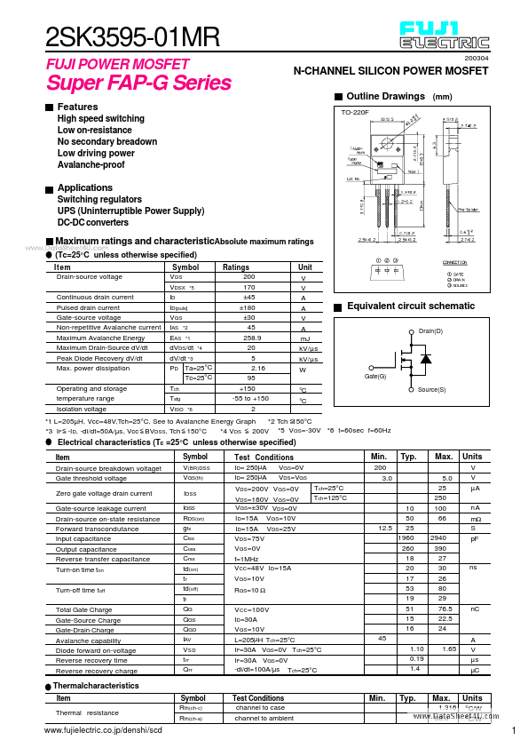
Outline Drawings (mm)
TO-220F
Applications
Switching regulators UPS (Uninterruptible Power Supply) DC-DC converters
..
Maximum ratings and characteristic Absolute maximum ratings
(Tc=25°C unless otherwise specified)
Symbol V DS VDSX
- 5 ID ID(puls] VGS IAS
- 2 EAS
- 1 d VDS/dt
- 4 d V/dt
- 3 PD Ta=25°C Tc=25°C Tch Tstg VISO Ratings 200 170 ±45 ±180 ±30 45 258.9 20 5 2.16 95 +150 -55 to +150 2 Unit V V A A V A m J k V/µs k V/µs W °C °C
Item Drain-source voltage Continuous drain current Pulsed drain current Gate-source voltage Non-repetitive Avalanche current Maximum Avalanche Energy Maximum Drain-Source d V/dt Peak Diode Recovery d V/dt Max. power dissipation Operating and storage temperature range Isolation voltage
Equivalent circuit schematic
Drain(D)
Gate(G) Source(S)
- 6
- 1 L=205µH, Vcc=48V,Tch=25°C, See to Avalanche Energy Graph
- 2 Tch < 150°C = < < < <
- 3 IF = -ID, -di/dt=50A/µs, Vcc = BVDSS, Tch = 150°C
- 4 VDS = 200V
- 5 VGS=-30V
- 6 t=60sec f=60Hz
Electrical characteristics (Tc =25°C unless otherwise specified)
Item Drain-source breakdown voltaget Gate threshold voltage Zero gate voltage drain current Gate-source leakage current Drain-source on-state resistance Forward transcondutance Input capacitance Output capacitance Reverse transfer capacitance Turn-on time ton Turn-off time toff Total Gate Charge Gate-Source Charge Gate-Drain Charge Avalanche capability Diode forward on-voltage Reverse recovery time Reverse recovery charge Symbol V(BR)DSS VGS(th) IDSS IGSS RDS(on) gfs Ciss Coss Crss td(on) tr td(off) tf QG QGS QGD IAV V SD t rr Qrr Test Conditions ID= 250µA VGS=0V ID= 250µA VDS=VGS VDS=200V VGS=0V VDS=160V VGS=0V VGS=±30V VDS=0V ID=15A VGS=10V ID=15A VDS=25V VDS =75V VGS=0V f=1MHz VCC=48V ID=15A VGS=10V RGS=10 Ω V CC=100V ID=30A VGS=10V L=205µH Tch=25°C IF=30A VGS=0V Tch=25°C IF=30A VGS=0V -di/dt=100A/µs Tch=25°C Tch=25°C...