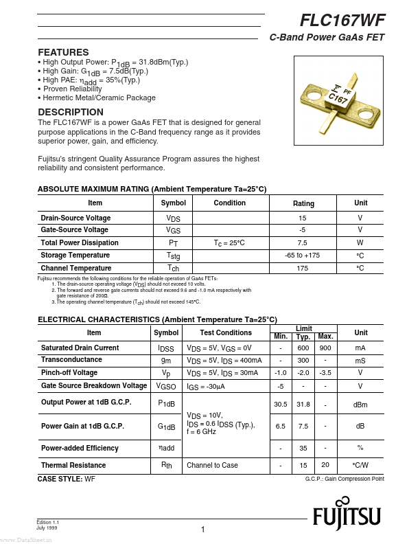
FLC167WF
FLC167WF is C-Band Power GaAs FET manufactured by Fujitsu Component.
FEATURES
- -
- -
- High Output Power: P1d B = 31.8d Bm(Typ.) High Gain: G1d B = 7.5d B(Typ.) High PAE: ηadd = 35%(Typ.) Proven Reliability Hermetic Metal/Ceramic Package
DESCRIPTION
The FLC167WF is a power Ga As FET that is designed for general purpose applications in the C-Band frequency range as it provides superior power, gain, and efficiency. Fujitsu’s stringent Quality Assurance Program assures the highest reliability and consistent performance. ABSOLUTE MAXIMUM RATING (Ambient Temperature Ta=25°C)
Item Drain-Source Voltage Gate-Source Voltage Total Power Dissipation Storage Temperature Channel Temperature Symbol VDS VGS PT Tstg Tch Tc = 25°C Condition Rating 15 -5 7.5 -65 to +175 175 Unit V V W °C °C
Fujitsu remends the following conditions for the reliable operation of Ga As FETs: 1. The drain-source operating voltage (VDS) should not exceed 10 volts. 2. The forward and reverse gate currents should not exceed 9.6 and -1.0 m A respectively with gate resistance of 200Ω. 3. The operating channel temperature (Tch) should not exceed 145°C.
ELECTRICAL CHARACTERISTICS (Ambient Temperature Ta=25°C)
Item Saturated Drain Current Transconductance Pinch-off Voltage Gate Source Breakdown Voltage Output Power at 1d B G.C.P. Symbol IDSS gm Vp VGSO P1d B G1d B ηadd Rth Channel to Case VDS = 10V, IDS = 0.6 IDSS (Typ.), f = 6 GHz Test Conditions VDS = 5V, VGS = 0V VDS = 5V, IDS = 400m A VDS = 5V, IDS = 30m A IGS = -30µA Min. -1.0 -5 30.5 6.5 Limit Typ. Max. 600 300 -2.0 31.8 7.5 35 15 900 -3.5 20 Unit m A m S V V d Bm d B % °C/W
Power Gain at 1d B G.C.P. Power-added Efficiency Thermal Resistance CASE STYLE: WF
G.C.P.: Gain pression Point
Edition 1.1 July 1999
.Data Sheet.in
C-Band Power Ga As FET
POWER DERATING CURVE 10 DRAIN CURRENT vs. DRAIN-SOURCE VOLTAGE
Total Power Dissipation (W)
Drain Current (m A)
8 6 4 2
VGS =0V -0.5V
-1.0V
-1.5V -2.0V
50 100 150 200
Case Temperature (°C)
OUTPUT POWER & IM3 vs. INPUT POWER
Drain-Source...