MB84VD2119xA Description
”) Host system can program or erase in one bank, then immediately and simultaneously read from the other bank Zero latency between read and write operations Read-while-erase Read-while-program Minimum 100,000 write/erase cycles Sector erase architecture Eight 4 K words and thirty one 32 K words. Any bination of sectors can be concurrently erased. Also supports full chip erase.
MB84VD2119xA Key Features
- Power supply voltage of 2.7 V to 3.6 V
- High performance 85 ns maximum access time
- Operating Temperature -25 °C to +85 °C
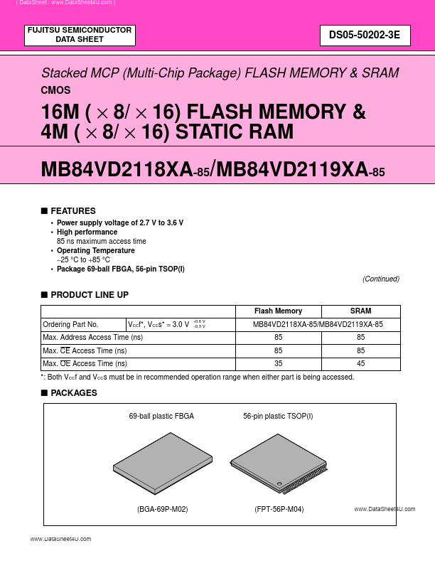
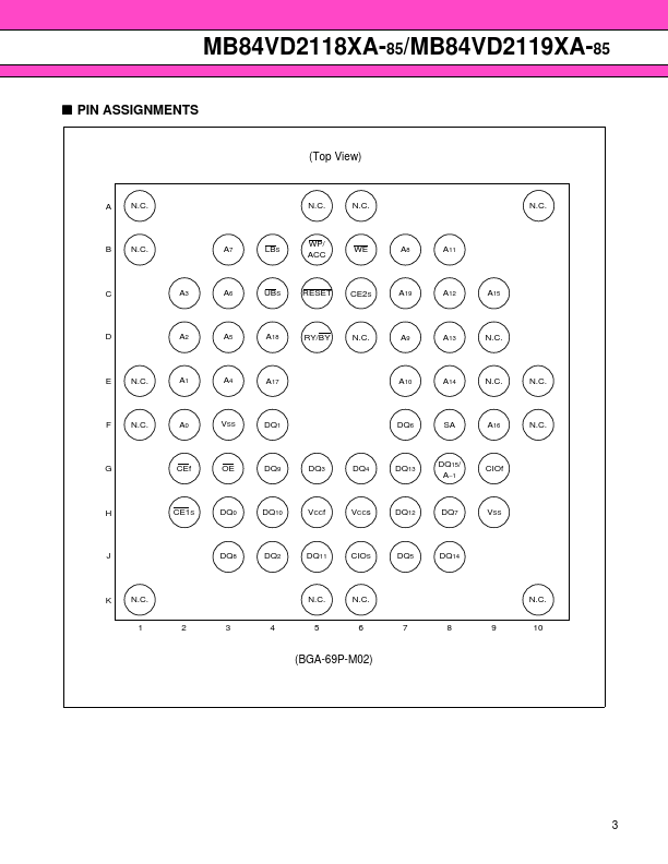
- Package 69-ball FBGA, 56-pin TSOP(I)
- Both VCCf and VCCs must be in remended operation range when either part is being accessed
- Simultaneous Read/Write operations (dual bank) Multiple devices available with different bank sizes (Refer to “PIN DESCR
- Minimum 100,000 write/erase cycles
- Sector erase architecture Eight 4 K words and thirty one 32 K words. Any bination of sectors can be concurrently erased.
- Boot Code Sector Architecture MB84VD2118XA : Top sector MB84VD2119XA : Bottom sector
- Embedded EraseTM- Algorithms Automatically pre-programs and erases the chip or any sector