MB86626 Description
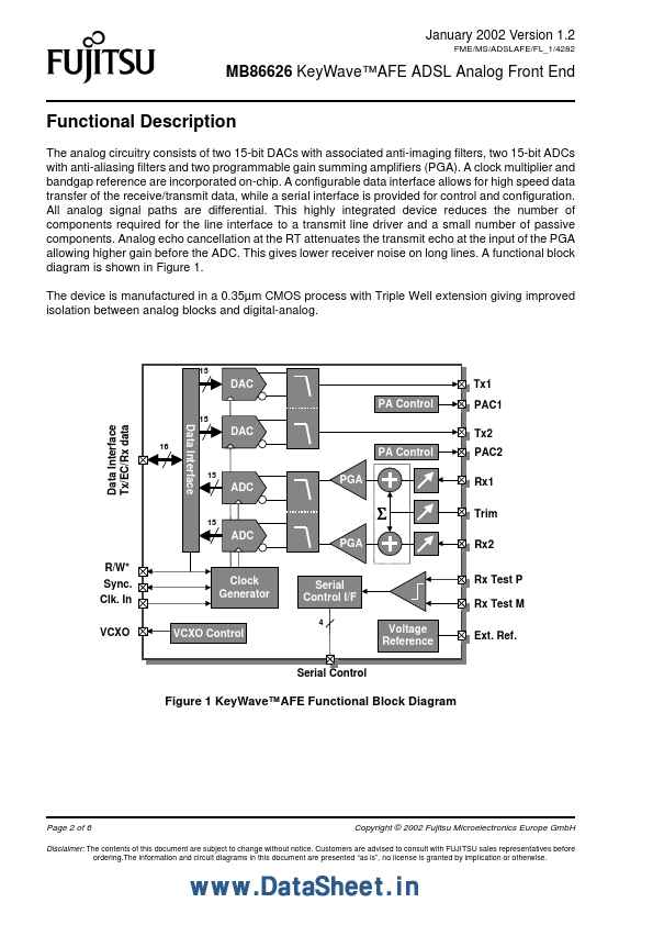
The analog circuitry consists of two 15-bit DACs with associated anti-imaging filters, two 15-bit ADCs with anti-aliasing filters and two programmable gain summing amplifiers (PGA). A clock multiplier and bandgap reference are incorporated on-chip. A configurable data interface allows for high speed data transfer of the receive/transmit data, while a serial interface is provided for control and configuration.
MB86626 Key Features
- Integrates all active circuits except transmit line driver
- Programmable for G.dmt (1 channel) or G.lite (2 channel)
- Low power, 3.3V operation
- from 235mW/ch (2 channel CO G.lite) to 525mW (RT G.dmt)
- Integrated filters and 15-bit A/D & D/A converters
- 0 to +38 dB AGC range for receive channel
- Supports analog and digital echo cancellation
- Excellent SFDR and input noise
- 0.35µm CMOS technology with Triple Well
- Industrial temperature range (-40 °C to +85 °C)