MBM29DL323BE
MBM29DL323BE is FLASH MEMORY CMOS 32 M (4 M X 8/2 M X 16) BIT manufactured by Fujitsu Semiconductor Limited.
- Part of the MBM29DL32xTE comparator family.
- Part of the MBM29DL32xTE comparator family.
DESCRIPTION
The MBM29DL32XTE/BE are a 32 M-bit, 3.0 V-only Flash memory organized as 4 Mbytes of 8 bits each or 2 Mwords of 16 bits each. These devices are designed to be programmed in-system with the standard system 3.0 V VCC supply. 12.0 V VPP and 5.0 V VCC are not required for write or erase operations. The devices can also be reprogrammed in standard EPROM programmers. MBM29DL32XTE/BE are organized into two banks, Bank 1 and Bank 2, which are considered to be two separate memory arrays for operations. It is the Fujitsu’s standard 3 V only Flash memories, with the additional capability of allowing a normal non-delayed read access from a non-busy bank of the array while an embedded write (either a program or an erase) operation is simultaneously taking place on the other bank. (Continued) s PRODUCT LINE UP
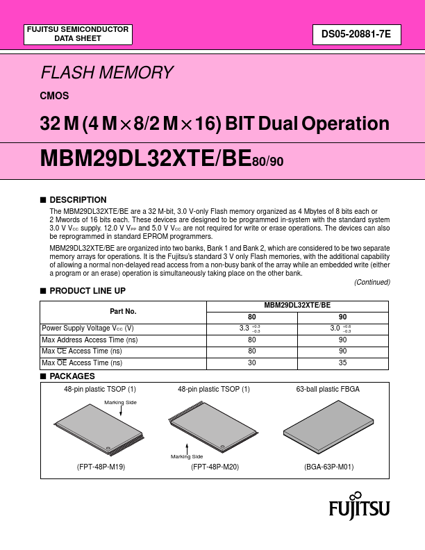
Part No. Power Supply Voltage VCC (V) Max Address Access Time (ns) Max CE Access Time (ns) Max OE Access Time (ns) MBM29DL32XTE/BE 80 3.3
+0.3
- 0.3
90 3.0
+0.6
- 0.3
80 80 30
90 90 35 s PACKAGES
48-pin plastic TSOP (1)
Marking Side
48-pin plastic TSOP (1)
63-ball plastic FBGA
Marking Side
(FPT-48P-M19)
(FPT-48P-M20)
(BGA-63P-M01)
MBM29DL32XTE/BE80/90
(Continued)
In the MBM29DL32XTE/BE, a new design concept is implemented, so called “Sliding Bank Architecture”. Under this concept, the MBM29DL32XTE/BE can be produced a series of devices with different Bank 1/Bank 2 size binations; 4 Mb/28 Mb, 8 Mb/24 Mb, 16 Mb/16 Mb. To eliminate bus contention the devices have separate chip enable (CE) , write enable (WE) , and output enable (OE) controls. The MBM29DL32XTE/BE are pin and mand set patible with JEDEC standard E2PROMs. mands are written to the mand register using standard microprocessor write timings. Register contents serve as input to an internal state-machine which controls the erase and programming circuitry. Write cycles also internally latch addresses and data needed for the programming and erase operations. Typically, each sector can be programmed...