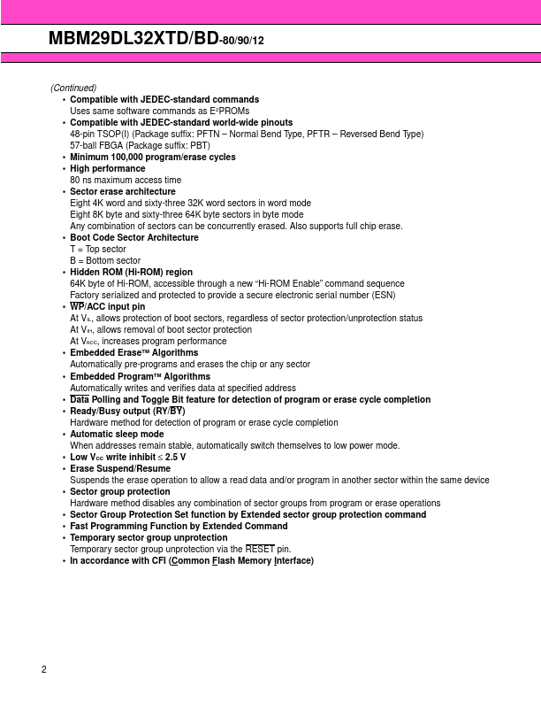
Datasheet4U Logo Datasheet4U.com

MBM29DL32xTD - 32M (4M X 8/2M X 16) BIT Dual Operation

Download the MBM29DL32xTD datasheet PDF. This datasheet also covers the MBM29DL32xBD variant, as both devices belong to the same 32m (4m x 8/2m x 16) bit dual operation family and are provided as variant models within a single manufacturer datasheet.

Description

The MBM29DL32XTD/BD are a 32M-bit, 3.0 V-only Flash memory organized as 4M bytes of 8 bits each or 2M words of 16 bits each.

The MBM29DL32XTD/BD are offered in a 48-pin TSOP(I) and FBGA Package.

These devices are designed to be programmed in-system with the standard system 3.0 V VCC supply.

Features

  • -80/90/12.
  • 0.33 µm Process Technology.
  • Simultaneous Read/Write operations (dual bank) Multiple devices available with different bank sizes (Refer to Table 1) Host system can program or erase in one bank, then immediately and simultaneously read from the other bank Zero latency between read and write operations Read-while-erase Read-while-program.
  • Single 3.0 V read, program, and erase Minimizes system level power requirements (Continued) s.

📥 Download Datasheet

Note: The manufacturer provides a single datasheet file (MBM29DL32xBD_FujitsuMediaDevices.pdf) that lists specifications for multiple related part numbers.

Full PDF Text Transcription

Click to expand full text
FUJITSU SEMICONDUCTOR DATA SHEET DS05-20873-4E FLASH MEMORY CMOS 32M (4M × 8/2M × 16) BIT Dual Operation MBM29DL32XTD/BD s FEATURES -80/90/12 • 0.33 µm Process Technology • Simultaneous Read/Write operations (dual bank) Multiple devices available with different bank sizes (Refer to Table 1) Host system can program or erase in one bank, then immediately and simultaneously read from the other bank Zero latency between read and write operations Read-while-erase Read-while-program • Single 3.0 V read, program, and erase Minimizes system level power requirements 
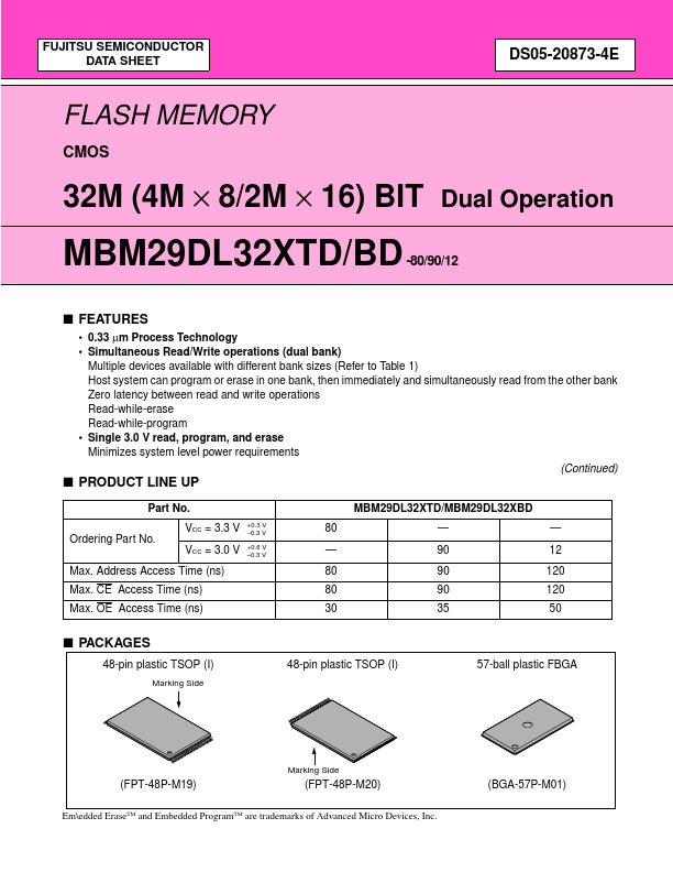
(Continued) s PRODUCT LINE UP Part No. VCC = 3.3 V Ordering Part No. VCC = 3.0 V Max. Address Access Time (ns) Max. CE Access Time (ns) Max. OE Access Time (ns) +0.3 V –0.3 V +0.6 V –0.
Published: |