MBM29SL800TE
MBM29SL800TE is FLASH MEMORY CMOS 8 M (1 M X 8/512 K X 16) BIT manufactured by Fujitsu Semiconductor Limited.
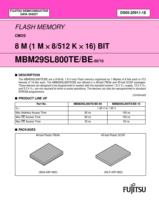
DESCRIPTION
The MBM29SL800TE/BE are a 8 M-bit, 1.8 V-only Flash memory organized as 1 Mbytes of 8 bits each or 512 Kwords of 16 bits each. The MBM29SL800TE/BE are offered in a 48-ball FBGA and 45-ball SCSP packages. These devices are designed to be programmed in-system with the standard system 1.8 V VCC supply. 12.0 V VPP and 5.0 V VCC are not required for write or erase operations. The devices can also be reprogrammed in standard EPROM programmers. (Continued) s PRODUCT LINE UP
Part No. VCC Max Address Access Time Max CE Access Time Max OE Access Time 90 ns 90 ns 30 ns MBM29SL800TE/BE-90 MBM29SL800TE/BE-10 100 ns 100 ns 35 ns 1.65 V to 1.95 V s PACKAGES
48-ball Plastic FBGA 45-ball Plastic SCSP
(BGA-48P-M20)
(WLP-45P-M02)
MBM29SL800TE/BE-90/10
(Continued)
The standard MBM29SL800TE/BE offer access times 90 ns and 100 ns, allowing operation of high-speed microprocessors without wait states. To eliminate bus contention the devices have separate chip enable (CE) , write enable (WE) , and output enable (OE) controls. The device supports pin and mand set patible with JEDEC standard E2PROMs. mands are written to the mand register using standard microprocessor write timings. Register contents serve as input to an internal state-machine which controls the erase and programming circuitry. Write cycles also internally latch addresses and data needed for the programming and erase operations. Reading data out of the devices is similar to reading from 5.0 V and 12.0 V Flash or EPROM devices. The device is programmed by executing the program mand sequence. This will invoke the Embedded Program Algorithm which is an internal algorithm that automatically times the program pulse widths and verifies proper cell margin. Typically, each sector can be programmed and verified in about 0.5 seconds. Erase is acplished by executing the erase mand sequence. This will invoke the Embedded Erase Algorithm which is an internal algorithm that automatically preprograms the array if it is not...