Fujitsu MB85R1002A
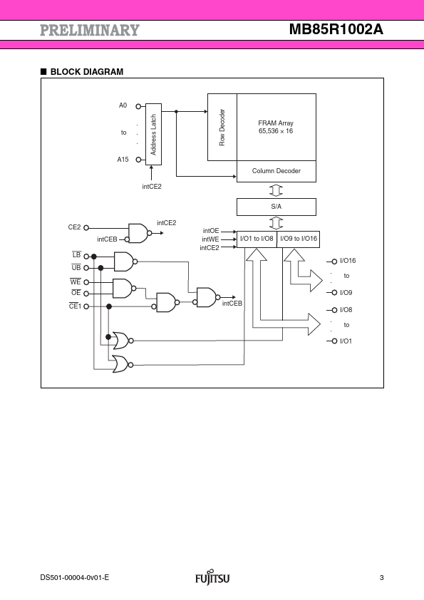
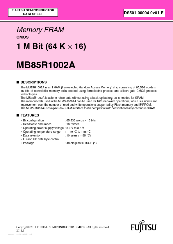
The MB85R1002A is an FRAM (Ferroelectric Random Access Memory) chip consisting of 65,536 words × 16 bits of nonvolatile memory cells created using ferroelectric process and silicon gate CMOS process technologies. The MB85R1002A is able to retain data without using a back-up battery, as is needed for SRAM. The memory cells used in the MB85R1002A can be used for 1010 read/write operations, which is a significant improvement over the number of read and write operations supported by Flash memory and E2PROM.| Part No. | MB85R1002A |
|---|---|
| Datasheet | MB85R1002A Download |
| Manufacturer |  Fujitsu |
| Description | 1 M Bit (64 K x 16) |
| Buy | Stock & Price |
FEATURES
●●
●
●
●
●
● Bit configuration Read/write endurance Operating power supply voltage Operating temperature range Data retention LB and UB data byte control Package : 65,536 words × 16 bits : 1010 times : 3.0 V to 3.6 V : − 40 °C to + 85 °C : 10 years ( + 55 °C) : 48-pin plastic TSOP (1) Copyright©2011 FUJITSU SEMICONDUCTOR LIMITED All rights reserved 2011.1 MB85R1002A
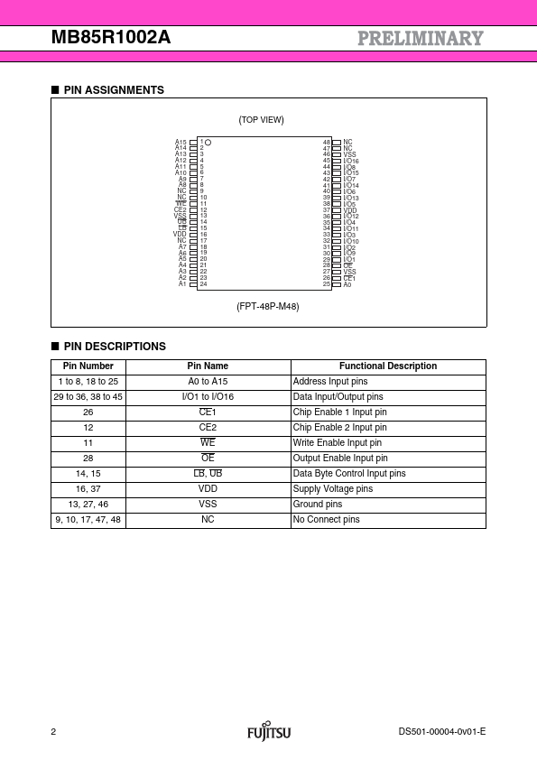
● PIN ASSIGNMENTS (TOP VIEW) A15 A14 A13 A12 A11 A10 A9 A8 NC NC WE CE2 VSS UB LB VDD NC A7 A6 A5 A4 A3 A2 A1 1 2 3 4 5 6 7 8 9 10 11 12 13 14 15 16 17 18 19 20 21 22 23 24 48 47 46 45 44 43 42 41 40 39 38 37 36 35 34 33 32 31 30 29 28 27 26 25 NC NC VSS I/O16 I/O8 I/O15 I/O7 I/O14 I/O6 I/O13 I/O5 VDD I/O12 I/O4 I/O11 I/O3 I/O10 I/O2 I/O9 I/O1 OE VSS CE1 A0 (FPT-48P-M48)
● PIN DESCRIPTIONS Pin Number 1 to 8, 18 to 25 29 to 36, 38 to 45 26 12 11 28 14, 15 16, 37 13, 27, 46 9, 10, 17, 47, 48 Pin Name A0 to A15 I/O1 to I/O16 CE1 CE2 WE OE LB, UB VDD VSS NC Functional
DESCRIPTION
Address Input pins Data Input/Output p...