MBM29DL164BD-70
MBM29DL164BD-70 is FLASH MEMORY CMOS 16M (2M x 8/1M x 16) BIT manufactured by Fujitsu Semiconductor Limited.
- Part of the MBM29DL16xTD comparator family.
- Part of the MBM29DL16xTD comparator family.
FEATURES
- 0.33 µm Process Technology
- Simultaneous Read/Write operations (dual bank)
Multiple devices available with different bank sizes (Refer to “MBM29DL16XTD/BD Device Bank Divisions Table” in s GENERAL DESCRIPTION
)
Host system can program or erase in one bank, then immediately and simultaneously read from the other bank
Zero latency between read and write operations
Read-while-erase
Read-while-program
- Single 3.0 V read, program, and erase
Minimizes system level power requirements s PRODUCT LINE UP
(Continued)
Part No.
Ordering Part No.
=
V +0.3 V
- 0.3 V
=
V +0.6 V
- 0.3 V
Max Address Access Time (ns)
Max CE Access Time (ns)
Max OE Access Time (ns)
MBM29DL16XTD/MBM29DL16XBD 70
- - 90 70 90 70 90 30 35 s PACKAGES
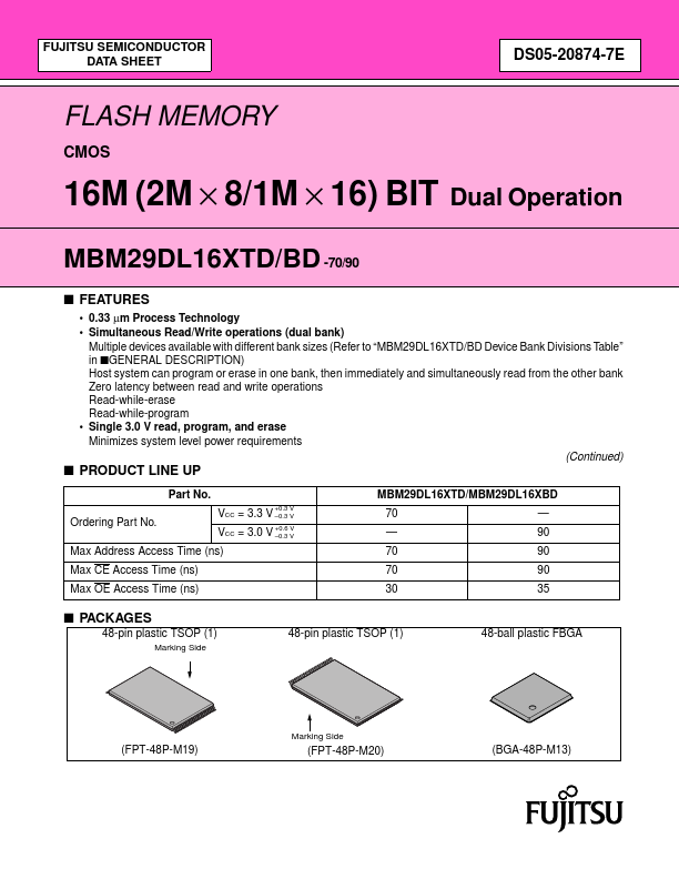
48-pin plastic TSOP (1)
Marking Side
48-pin plastic...