Datasheet4U.com
🌙
MBM29DL322BD-12 Datasheet | Fujitsu Semiconductor Limited
Part:
MBM29DL322BD-12
Description:
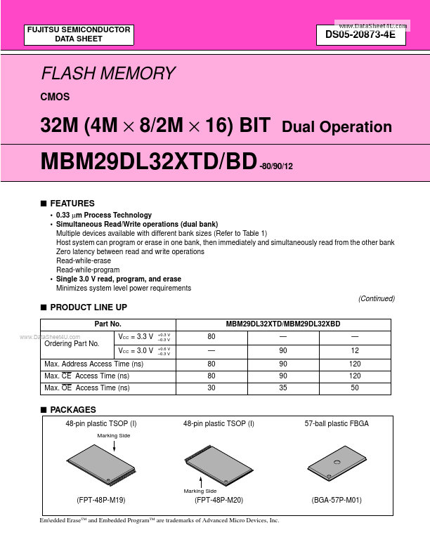
32M (4M x 8/2M x 16) BIT Dual Operation
Manufacturer:
Fujitsu Semiconductor Limited
Size:
1.58 MB
MBM29DL322BD-12 Datasheet (PDF) Download
Fujitsu Semiconductor Limited
MBM29DL322BD-12
Key Features
0.33 µm Process Technology
Simultaneous Read/Write operations (dual bank) Multiple devices available with different bank sizes (Refer to Table
×
Close