MBM29F400BC-70 Key Features
- Single 5.0 V read, write, and erase Minimizes system level power requirements
- patible with JEDEC-standard mands Uses same software mands as E2PROMs
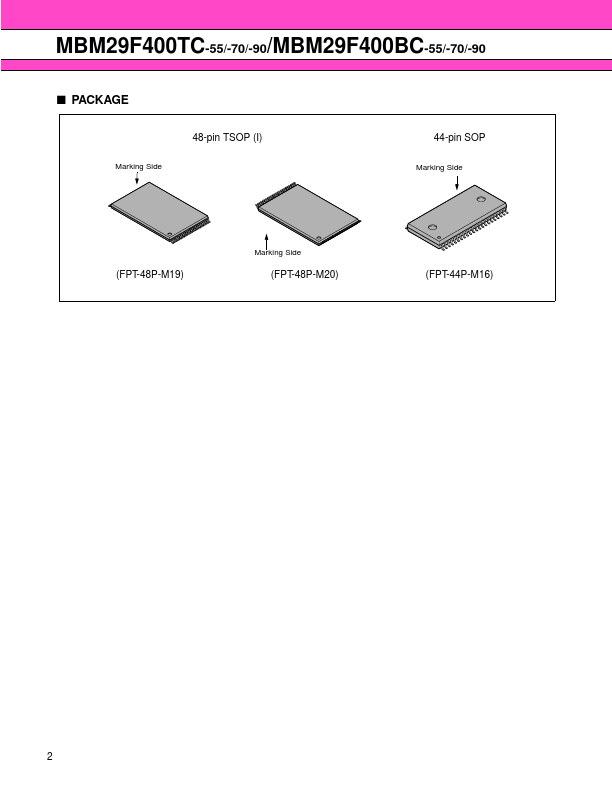
- patible with JEDEC-standard world-wide pinouts 48-pin TSOP (Package suffix: PFTN
- Normal Bend Type, PFTR
- Reversed Bend Type) 44-pin SOP (Package suffix: PF)
- Minimum 100,000 write/erase cycles
- High performance
- Sector erase architecture
- Boot Code Sector Architecture T = Top sector B = Bottom sector
- Embedded EraseTM Algorithms Automatically pre-programs and erases the chip or any sector