MBM29LV080A-90 Overview
Key Features
- Address specification is not necessary during command sequence
- Single 3.0 V read, program and erase Minimizes system level power requirements
- Compatible with JEDEC-standard commands Uses same software commands as E2PROMs
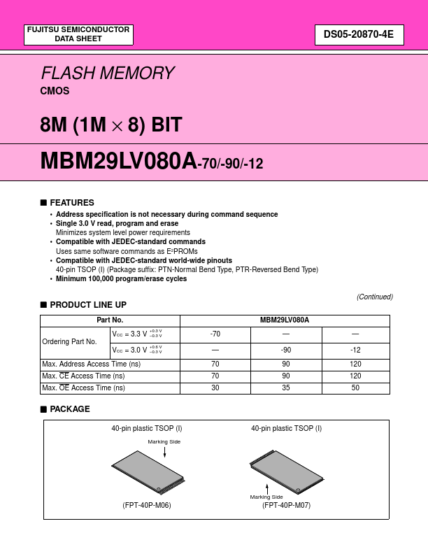
- Compatible with JEDEC-standard world-wide pinouts 40-pin TSOP (I) (Package suffix: PTN-Normal Bend Type, PTR-Reversed Bend Type)
- 70 70 30 MBM29LV080A
- High performance 70 ns maximum access time