DESCRIPTION
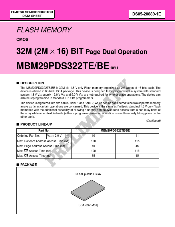
10/11 The device is offered in 63-ball FBGA package. 12.0 V VPP and 5.0 V VCC are not required for write or erase operations. The device can also be reprogrammed in standard EPROM programmers. The device is organized into two banks, Bank 1 and Bank 2, which can be considered to be two separate memory arrays as far as certain operations are concerned. This device is the same as Fujitsu’s standard 1.8 V only Flash memories with the additional capability of allowing a normal non-delayed read access from a non-busy bank of the array while an embedded write (either a program or an erase) operation is simultaneously taking place on the other bank. (Continued) s PRODUCT LINE-UP Part No. Ordering Part No. VCC = 2.0 V +0.2 V –0.2 V MBM29PDS322TE/BE 10 100 45 100 35 11 115 45 115 45 Max. Random Address Access Time (ns) Max. Page Address Access Time (ns) Max. CE Access Time (ns) Max. OE Access Time (ns) s PACKAGE 63-ball plastic FBGA (BGA-63P-M01) MBM29PDS322TE/BE 10/11 (Continued) The device provides truly high performance non-volatile Flash memory solution. Fujitsu