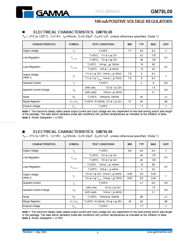
ELECTRICAL CHARACTERISTICS
GM78L05 TA = 0°C to 125º C, VI=10V, IO=40mA, CI=0.33µF, unless otherwise specified (Note 1) CHARACTERISTICS Output Voltage Line Regulation SYMBOL VO VR LINE VR LOAD VO IQ ∆IQ NO ∆VI /∆VO V DO (with Line) (with Load) TEST CONDITIONS TJ=25°C TJ=25°C, 7V ≤ VI ≤ 20V TJ=25°C, 8V ≤ VI ≤ 20V TJ=25°C, 1mA ≤ I O ≤ 100mA TJ=25°C, 1mA ≤ I O ≤ 40mA 7V ≤ VI ≤ 20V, 1mA ≤ I O ≤ 40mA 7V ≤ VI ≤ VMAX, 1mA ≤ I O ≤ 70mA TJ=25°C 8V ≤ V I ≤ 2 0 V 1mA ≤ I O ≤ 40mA 42 41 49 1.7 4.75 4.75 MIN 4.8 TYP 5.0 32 26 11 5 5 5 3.8 MAX 5.2 150 100 60 30 5.25 5.25 6.0 1.5 0.1 UNIT V mV Load Regulation Output Voltage (Note 2) Quiscent Current Quiscent Current Change Noise Ripple Rejection Dropout Voltage mV V mA mA µV dB V TA=25°C, 10Hz ≤ f ≤ 100kHz TJ=25°C, f=120kHz, 8V ≤ VI ≤ 18V TJ=25°C Note 1: The maximum steady state usable output current and input voltage are very dependent on the heat sinking and/or lead length of the package. The data above represent pulse test conditions with junction temperatures as indicated at the initiation of tests.