BD038
Overview
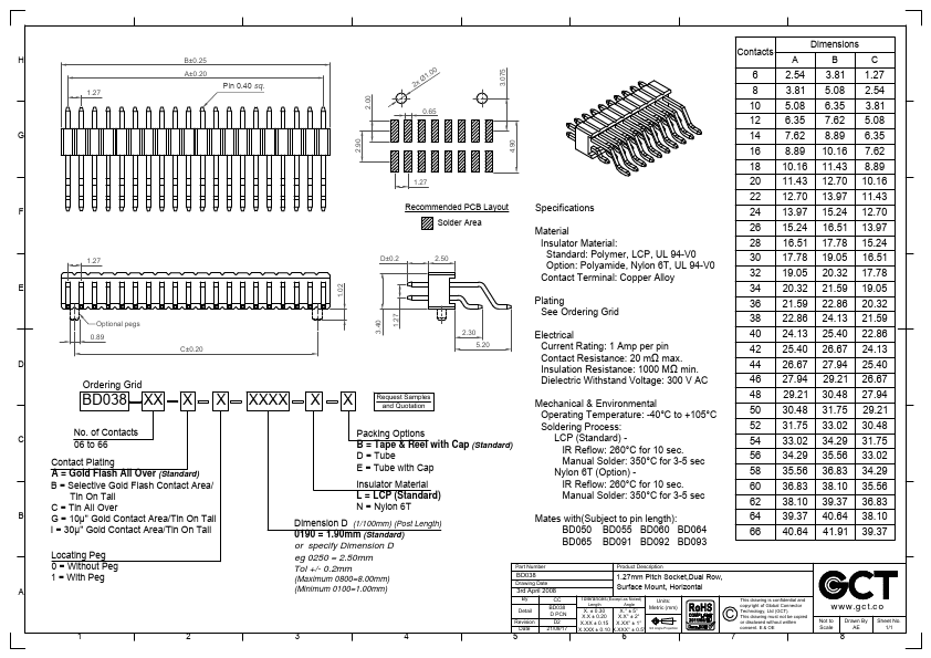
2.90 2.00 3.075 4.90 H 1.27 B±0.25 A±0.20 Pin 0.40 sq. 2x Ø1.00 0.65 Contacts 6 8 10 12 Dimensions A B C 2.54 3.81 1.27 3.81 5.08 2.54 5.08 6.35 3.81 6.35 7.62 5.08 G 14 7.62 8.89 6.35 ...
| Part | BD038 |
|---|---|
| Description | 1.27mm Pitch Socket |
| Manufacturer | GCT |
| Size | 72.45 KB |
2.90 2.00 3.075 4.90 H 1.27 B±0.25 A±0.20 Pin 0.40 sq. 2x Ø1.00 0.65 Contacts 6 8 10 12 Dimensions A B C 2.54 3.81 1.27 3.81 5.08 2.54 5.08 6.35 3.81 6.35 7.62 5.08 G 14 7.62 8.89 6.35 ...
| Part Number | Manufacturer | Description |
|---|---|---|
| BD034 | Jiangsu Changjiang Electronics | TRANSISTOR |
| LXHL-BD03 | luxeon | Luxeon Emitter |
| BD034 | SeCoS Halbleitertechnologie GmbH | PNP General Purpose Transistor |