GENESYS LOGIC GL819
USB 2.0 Generation 3 Multi-I/F Card Reader Controller
| Part No. | GL819 |
|---|---|
| Datasheet | GL819 Download |
| Manufacturer |  GENESYS LOGIC |
| Description | USB 2.0 Generation 3 Multi-I/F Card Reader Controller |
| Buy | Stock & Price |
DESCRIPTION
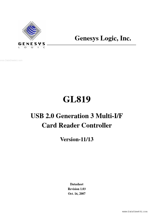
1. Pin List, Ch3.2, p.10 2. Pin Out, Ch3.3, p.11 3.ABSOLUTE MAXIMUM RATINGS
, Ch6.1, p16 4. DC Characteristics, Ch6.3, p.16 Remove over current protection support Modify: 1. SD Interface Timing, , Ch6.5.7, p.29, 30 2. SD_WP description, Table3.2, p.12 1.02 1.03 ©2000-2007 Genesys Logic Inc. - All rights reserved. Page 3 GL819 USB 2.0 Generation 3 Multi-I/F Card Reader Controller TABLE OF CONTENTS CHAPTER 1GENERAL DESCRIPTION
................................................... 7 CHAPTER 2FEATURES
.............................................................................. 8 CHAPTER 3 PIN ASSIGNMENT................................................................. 9 3.1 PINOUT ....................................................................................................... 9 3.2 PIN LIST.................................................................................................... 10 3.3 PIN DESCRIPTIONS ...................................................................................