High speed switching High Current High surge resisitivity for CRT discharge High reliability design High Voltage
APPLICATIONS
X light Power supply Laser Voltage doubler circuit Microwave emission power
MAXIMUM RATINGS
and Characteristics
ABSOLUTE MAXIMUM RATINGS
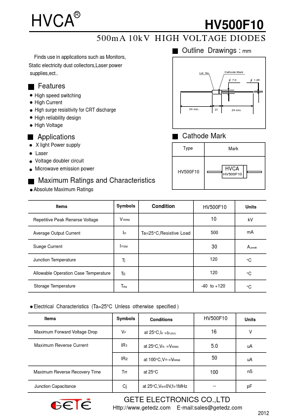
Outline Drawings : mm Lot No. Cathode Mark o 7.0 o 1.28 24 min. 21 24 min. Cathode Mark Type Mark HV500F10 HVCA HV500F10 Items Symbols Condition Repetitive Peak Renerse Voltage V RRM Average Output Current IO Ta=25°C,Resistive Load Suege Current I FSM Junction Temperature Tj Allowable Operation Case Temperature Storage Temperature Tc Tstg HV500F10 10 500 30 120 120 -40 to +120 Units kV mA A peak °C °C °C
ELECTRICAL CHARACTERISTICS
(Ta=25°C Unless otherwise specified ) Items Symbols Conditions Maximum Forward Voltage Drop VF at 25°
This website uses cookies or similar technologies, to enhance your browsing experience and provide personalized recommendations. By continuing to use our website, you agree to our Privacy Policy