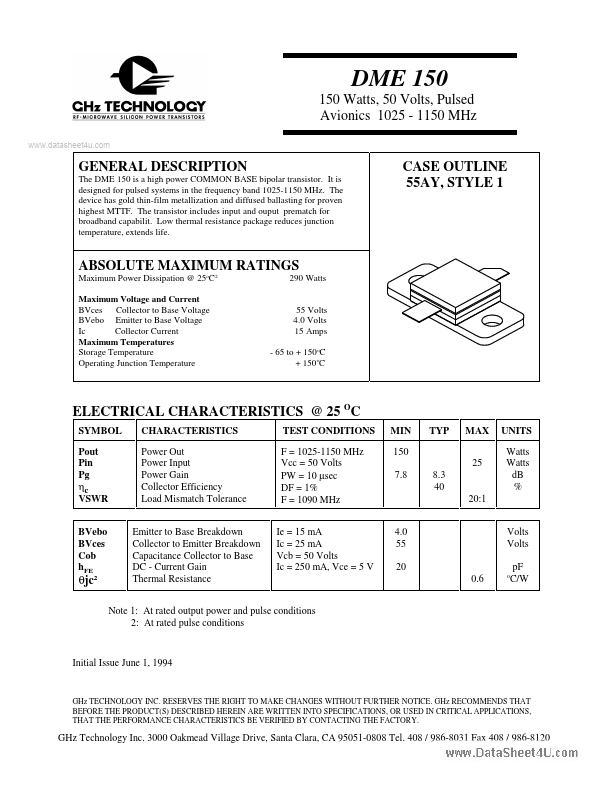
GENERAL DESCRIPTION
The device has gold thin-film metallization and diffused ballasting for proven highest MTTF. The transistor includes input and ouput prematch for broadband capabilit. Low thermal resistance package reduces junction temperature, extends life. CASE OUTLINE 55AY, STYLE 1 ABSOLUTE MAXIMUM RATINGS
Maximum Power Dissipation @ 25oC2 Maximum Voltage and Current BVces Collector to Base Voltage BVebo Emitter to Base Voltage Ic Collector Current Maximum Temperatures Storage Temperature Operating Junction Temperature 290 Watts 55 Volts 4.0 Volts 15 Amps - 65 to + 150 oC + 150 oC ELECTRICAL CHARACTERISTICS
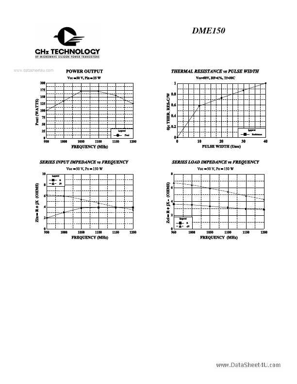
@ 25 OC SYMBOL Pout Pin Pg ηc VSWR BVebo BVces Cob hFE CHARACTERISTICS Power Out Power Input Power Gain Collector Efficiency Load Mismatch Tolerance Emitter to Base Breakdown Collector to Emitter Breakdown Capacitance Collector to Base DC - Current Gain Thermal Resistance TEST CONDITIONS F = 1025-1150 MHz Vcc = 50 Volts PW = 10 µsec DF = 1% F = 1090 MHz Ie = 15 mA Ic = 25 mA V... GHz Technology