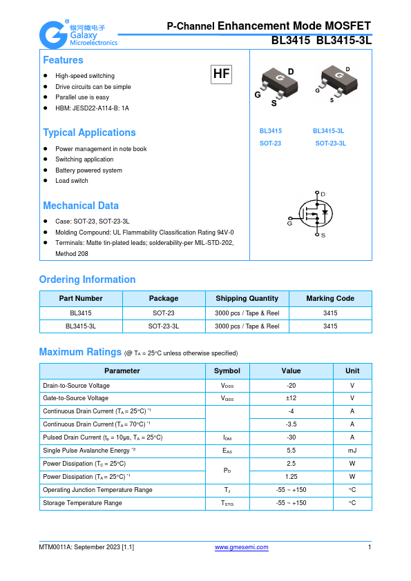
BL3415
Features
- High-speed switching
- Drive circuits can be simple
- Parallel use is easy
- HBM: JESD22-A114-B: 1A
P-Channel Enhancement Mode MOSFET BL3415 BL3415-3L
Typical Applications
- Power management in note book
- Switching application
- Battery powered system
- Load switch
BL3415 SOT-23
BL3415-3L SOT-23-3L
Mechanical Data
- Case: SOT-23, SOT-23-3L
- Molding pound: UL Flammability Classification Rating 94V-0
- Terminals: Matte tin-plated leads; solderability-per MIL-STD-202,
Method 208
Ordering Information
Part Number
BL3415 BL3415-3L
Package
SOT-23 SOT-23-3L
Shipping Quantity
3000 pcs / Tape & Reel 3000 pcs / Tape & Reel
Marking Code
3415 3415
Maximum Ratings (@ TA = 25°C unless otherwise specified)
Parameter
Drain-to-Source Voltage Gate-to-Source Voltage Continuous Drain Current (TA = 25°C)
- 1 Continuous Drain Current (TA = 70°C)
- 1 Pulsed Drain Current (tp = 10μs, TA = 25°C) Single Pulse Avalanche Energy
- 3 Power Dissipation (TC = 25°C) Power Dissipation (TA = 25°C)
-...