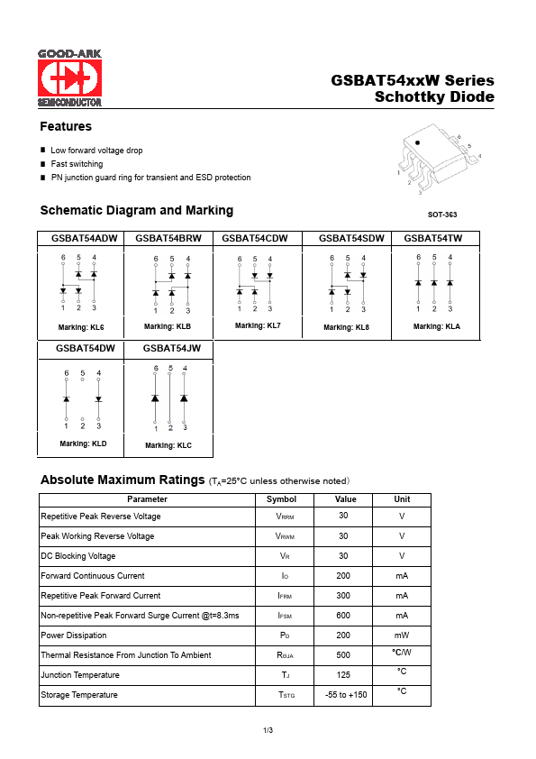
Download the GSBAT54DW datasheet PDF.
This datasheet also covers the GSBAT54ADW-GOOD variant, as both devices belong to the same schottky diode family and are provided as variant models within a single manufacturer datasheet.
Key Features
Low forward voltage drop.
Fast switching.
PN junction guard ring for transient and ESD protection
Schematic Diagram and Marking
GSBAT54ADW GSBAT54BRW GSBAT54CDW
GSBAT54xxW Series Schottky Diode
GSBAT54SDW
SOT-363
GSBAT54TW
Marking: KL6
GSBAT54DW
Marking: KLB
GSBAT54JW
Marking: KL7
Marking: KL8
Marking: KLA
Marking: KLD
Marking: KLC
Absolute Maximum Ratings (TA=25°C unless otherwise noted)
Parameter
Symbol
Value
Repetitive Peak Reverse Voltage
VRRM
30
Peak Workin.
Full PDF Text Transcription for GSBAT54DW (Reference)
Note: Below is a high-fidelity text extraction (approx. 800 characters) for
GSBAT54DW. For precise diagrams, and layout, please refer to the original PDF.
Features ■ Low forward voltage drop ■ Fast switching ■ PN junction guard ring for transient and ESD protection Schematic Diagram and Marking GSBAT54ADW GSBAT54BRW GSBAT54...
View more extracted text
protection Schematic Diagram and Marking GSBAT54ADW GSBAT54BRW GSBAT54CDW GSBAT54xxW Series Schottky Diode GSBAT54SDW SOT-363 GSBAT54TW Marking: KL6 GSBAT54DW Marking: KLB GSBAT54JW Marking: KL7 Marking: KL8 Marking: KLA Marking: KLD Marking: KLC Absolute Maximum Ratings (TA=25°C unless otherwise noted) Parameter Symbol Value Repetitive Peak Reverse Voltage VRRM 30 Peak Working Reverse Voltage VRWM 30 DC Blocking Voltage VR 30 Forward Continuous Current IO 200 Repetitive Peak Forward Current IFRM 300 Non-repetitive Peak Forward Surge Current @t=8.