GS8170DW72C
GS8170DW72C is Double Late Write SigmaRAM manufactured by GSI Technology.
- Part of the GS8170DW36C comparator family.
- Part of the GS8170DW36C comparator family.
Preliminary GS8170DW36/72C-333/300/250/200
209-Bump BGA mercial Temp Industrial Temp
18Mb Σ1x1Dp CMOS I/O
Double Late Write SigmaRAM™
200 MHz- 333 MHz 1.8 V VDD 1.8 V I/O
Features
- Double Late Write mode, Pipelined Read mode
- JEDEC-standard SigmaRAM™ pinout and package
- 1.8 V +150/- 100 mV core power supply
- 1.8 V CMOS Interface
- ZQ controlled user-selectable output drive strength
- Dual Cycle Deselect
- Burst Read and Write option
- Fully coherent read and write pipelines
- Echo Clock outputs track data output drivers
- Byte write operation (9-bit bytes)
- 2 user-programmable chip enable inputs
- IEEE 1149.1 JTAG-pliant Serial Boundary Scan
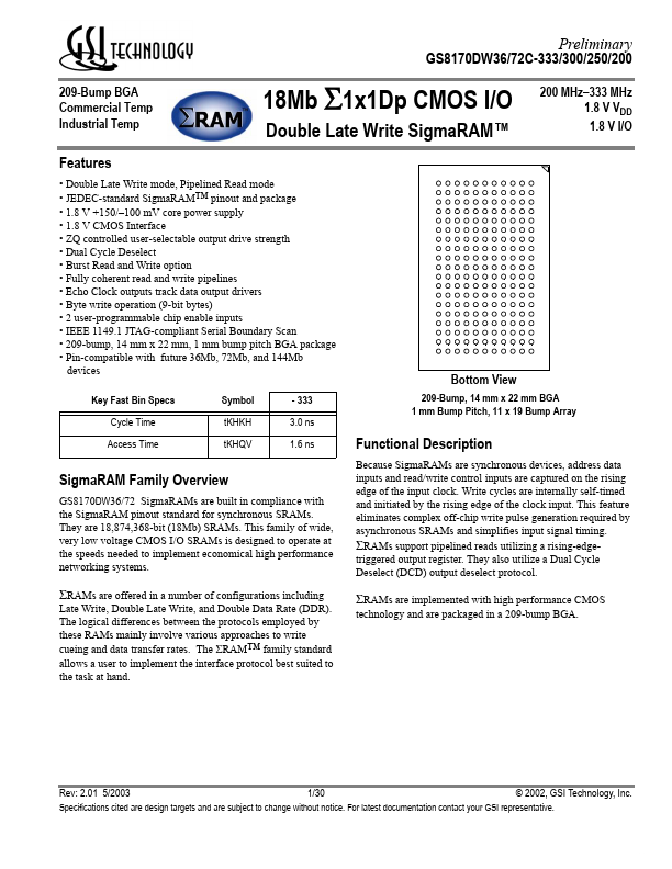
- 209-bump, 14 mm x 22 mm, 1 mm bump...