Datasheet4U Logo Datasheet4U.com

GS8182T19BD - 18Mb SigmaDDR-II+ Burst of 2 SRAM

Features

  • 2.0 Clock Latency.
  • Simultaneous Read and Write SigmaDDR-II™ Interface.
  • Common I/O bus.
  • JEDEC-standard pinout and package.
  • Double Data Rate interface.
  • Byte Write (x36 and x18) function.
  • Burst of 2 Read and Write.
  • 1.8 V +100/.
  • 100 mV core power supply.
  • 1.5 V or 1.8 V HSTL Interface.
  • Pipelined read operation with self-timed Late Write.
  • Fully coherent read and write pipelines.
  • ZQ pin f.

📥 Download Datasheet

Datasheet Details

Part number GS8182T19BD
Manufacturer GSI Technology
File Size 177.34 KB
Description 18Mb SigmaDDR-II+ Burst of 2 SRAM
Datasheet download datasheet GS8182T19BD Datasheet

Full PDF Text Transcription

Click to expand full text
GS8182T19/37BD-435/400/375/333/300
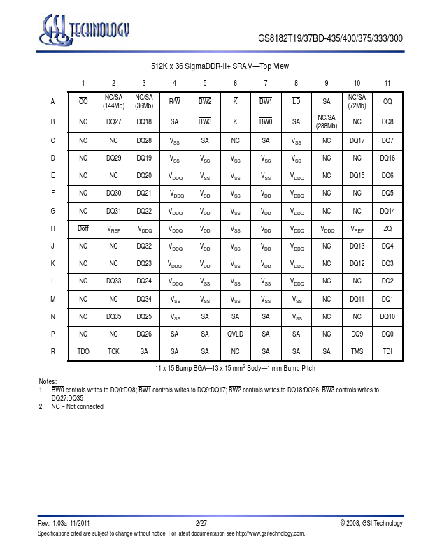
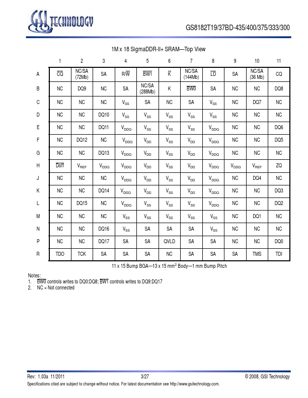
 165-Bump BGA Commercial Temp Industrial Temp 18Mb SigmaDDR-II+TM Burst of 2 SRAM 435 MHz–300 MHz 1.8 V VDD 1.8 V and 1.5 V I/O Features • 2.0 Clock Latency • Simultaneous Read and Write SigmaDDR-II™ Interface • Common I/O bus • JEDEC-standard pinout and package • Double Data Rate interface • Byte Write (x36 and x18) function • Burst of 2 Read and Write • 1.8 V +100/–100 mV core power supply • 1.5 V or 1.8 V HSTL Interface • Pipelined read operation with self-timed Late Write • Fully coherent read and write pipelines • ZQ pin for programmable output drive strength • IEEE 1149.
Published: |