GS8342Q10BGD Datasheet Text
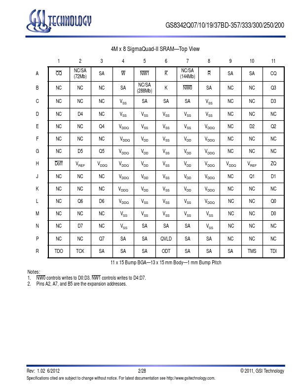
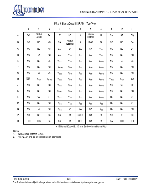
GS8342Q07/10/19/37BD-357/333/300/250/200
165-Bump BGA mercial Temp Industrial Temp
36Mb SigmaQuad-II+TM Burst of 2 SRAM
357 MHz- 200 MHz 1.8 V VDD
1.8 V and 1.5 V I/O
Features
- 2.0 Clock Latency
- Simultaneous Read and Write SigmaQuad™ Interface
- JEDEC-standard pinout and package
- Dual Double Data Rate interface
- Byte Write controls sampled at data-in time
- On-Die Termination (ODT) on Data (D), Byte Write (BW), and Clock (K, K) inputs
- Burst of 2 Read and Write
- 1.8 V +100/- 100 mV core power supply
- 1.5 V or 1.8 V HSTL Interface
- Pipelined read operation
- Fully coherent read and write pipelines
- ZQ pin for programmable output drive strength
- Data Valid Pin (QVLD) Support
- IEEE 1149.1 JTAG-pliant Boundary Scan
- 165-bump, 13 mm x 15 mm, 1 mm bump pitch BGA package
- RoHS-pliant 165-bump BGA package available
SigmaQuad™ Family Overview
The GS8342Q07/10/19/37BD are built in pliance with the SigmaQuad-II+ SRAM pinout standard for Separate I/O synchronous SRAMs. They are 37,748,736-bit (36Mb) SRAMs. The GS8342Q07/10/19/37BD SigmaQuad SRAMs are just one element in a family of low power, low voltage HSTL I/O SRAMs designed to operate at the speeds needed to implement economical high performance networking systems.
Clocking and Addressing Schemes
The GS8342Q07/10/19/37BD SigmaQuad-II+ SRAMs are synchronous devices. They employ two input register clock inputs, K and K. K and K are independent single-ended clock inputs, not differential inputs to a single differential clock input buffer.
Each internal read and write operation in a SigmaQuad-II+ B2 RAM is two times wider than the device I/O bus. An input data bus de-multiplexer is used to accumulate ining data before it is simultaneously written to the memory array. An output data multiplexer is...