GS8342T09E-333
Features
- Simultaneous Read and Write Sigma CIO™ Interface
- mon I/O bus
- JEDEC-standard pinout and package
- Double Data Rate interface
- Byte Write (x36 and x18) and Nybble Write (x8) function
- Burst of 2 Read and Write
- 1.8 V +100/- 100 m V core power supply
- 1.5 V or 1.8 V HSTL Interface
- Pipelined read operation with self-timed Late Write
- Fully coherent read and write pipelines
- ZQ pin for programmable output drive strength
- IEEE 1149.1 JTAG-pliant Boundary Scan
- 165-bump, 15 mm x 17 mm, 1 mm bump pitch BGA package
- Ro HS-pliant 165-bump BGA package available
- Pin-patible with present 9Mb and 18Mb and future 72Mb and 144Mb devices
36Mb Sigma CIO DDR-II Burst of 2 SRAM
167 MHz- 333 MHz 1.8 V VDD 1.8 V and 1.5 V I/O
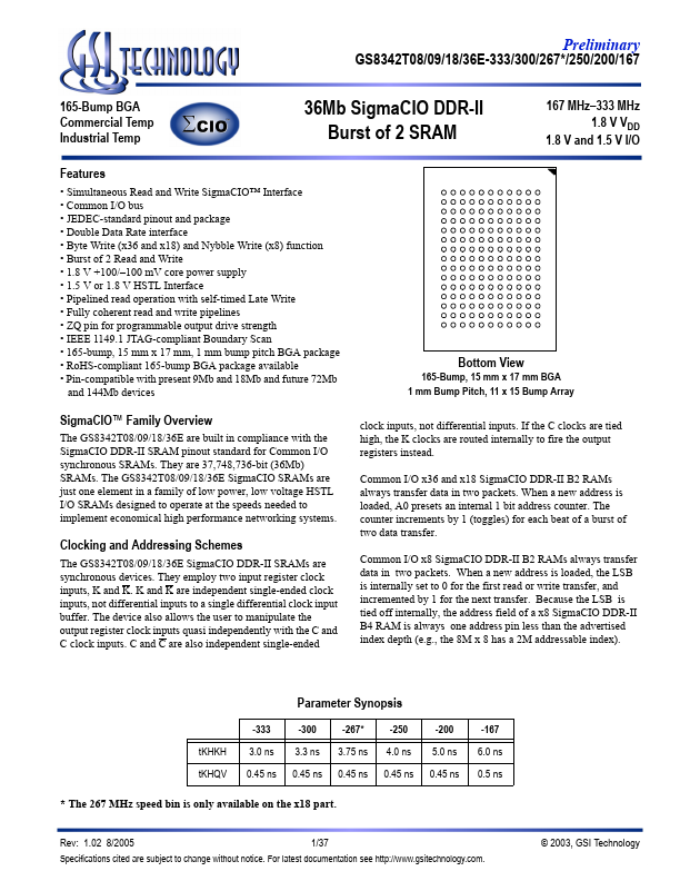
Bottom View
165-Bump, 15 mm x 17 mm BGA 1 mm Bump Pitch, 11 x 15 Bump Array clock inputs, not differential inputs. If the C clocks are tied high, the K clocks are routed internally to fire the output registers instead.
Sigma CIO™ Family Overview
The...