GS8342T18GE-300
GS8342T18GE-300 is 36Mb SigmaCIO DDR-II Burst SRAM manufactured by GSI Technology.
- Part of the GS8342T08E comparator family.
- Part of the GS8342T08E comparator family.
Preliminary GS8342T08/09/18/36E-333/300/267- /250/200/167
165-Bump BGA mercial Temp Industrial Temp Features
- Simultaneous Read and Write Sigma CIO™ Interface
- mon I/O bus
- JEDEC-standard pinout and package
- Double Data Rate interface
- Byte Write (x36 and x18) and Nybble Write (x8) function
- Burst of 2 Read and Write
- 1.8 V +100/- 100 m V core power supply
- 1.5 V or 1.8 V HSTL Interface
- Pipelined read operation with self-timed Late Write
- Fully coherent read and write pipelines
- ZQ pin for programmable output drive strength
- IEEE 1149.1 JTAG-pliant Boundary Scan
- 165-bump, 15 mm x 17 mm, 1 mm bump pitch BGA package
- Ro HS-pliant 165-bump BGA package available
- Pin-patible with present 9Mb and 18Mb and future 72Mb and 144Mb devices
36Mb Sigma CIO DDR-II Burst of 2 SRAM
167 MHz- 333 MHz 1.8 V VDD 1.8 V and 1.5 V I/O
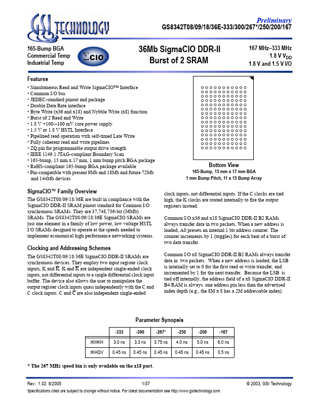
Bottom View
165-Bump, 15 mm x 17 mm BGA 1 mm Bump Pitch, 11 x 15 Bump Array clock inputs, not differential inputs. If the C clocks are tied high, the K clocks are routed internally to fire the output registers instead.
Sigma CIO™ Family Overview
The GS8342T08/09/18/36E are built in pliance with the Sigma CIO DDR-II SRAM pinout standard for mon I/O synchronous SRAMs. They are 37,748,736-bit (36Mb) SRAMs. The GS8342T08/09/18/36E Sigma CIO SRAMs are just one element in a family of low power, low voltage HSTL I/O SRAMs designed to operate at the speeds needed to implement economical high performance networking systems. http://..net/
Clocking and Addressing Schemes
The GS8342T08/09/18/36E Sigma CIO DDR-II SRAMs are synchronous devices. They employ two input register clock inputs, K and K. K and K are independent single-ended clock inputs, not differential inputs to a single differential clock input buffer. The device also allows the user to manipulate the output register clock inputs quasi independently with the C and C clock inputs. C and C are also independent single-ended mon I/O x36 and x18 Sigma CIO DDR-II...