GSI Technology GS8642Z18
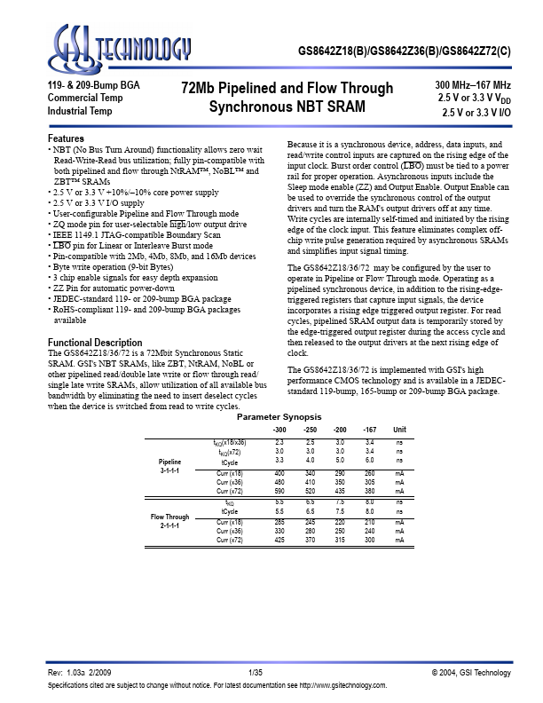
The GS8642Z18/36/72 may be configured by the user to operate in Pipeline or Flow Through mode. For read cycles, pipelined SRAM output data is temporarily stored by the edge-triggered output register during the access cycle and then released to the output drivers at the next rising edge of clock. The GS8642Z18/36/72 is implemented with GSI's high performance CMOS technology and is available in a JEDECstandard 119-bump, 165-bump or 209-bump BGA package.| Part No. | GS8642Z18 |
|---|---|
| Datasheet | GS8642Z18 Download |
| Manufacturer |  GSI Technology |
| Description | 72Mb Pipelined and Flow Through Synchronous NBT SRAM |
| Buy | Stock & Price |
FEATURES
● NBT (No Bus Turn Around) functionality allows zero wait Read-Write-Read bus utilization; fully pin-compatible with both pipelined and flow through NtRAM™, NoBL™ and ZBT™ SRAMs● 2.5 V or 3.3 V +10%/–10% core power supply
● 2.5 V or 3.3 V I/O supply
● User-configurable Pipeline and Flow Through mode
● ZQ mode pin for user-selectable high/low output drive
● IEEE 1149.1 JTAG-compatible Boundary Scan
● LBO pin for Linear or Interleave Burst mode
● Pin-compatible with 2Mb, 4Mb, 8Mb, and 16Mb devices
● Byte write operation (9-bit Bytes)
● 3 chip enable signals for easy depth expansion
● ZZ Pin for automatic power-down
● JEDEC-standard 119- or 209-bump BGA package
● Pb-Free 119- and 209-bump BGA packages available 72Mb Pipelined and Flow Through Synchronous NBT SRAM 300 MHz–167 MHz 2.5 V or 3.3 V VDD 2.5 V or 3.3 V I/O Because it is a synchronous device, address, data inputs, and read/write control inputs are captured on the rising edge of the input clock. Burst order control (LBO) must be tied to a power rail for proper operation.