Description
Address field LSBs and Address Counter Preset Inputs Address Inputs I/O Data Input and Output pins I I I - I I I I I I I I I I I Byte Write Enable for DQA, DQB I/Os; active low Byte Write Enable for DQC, DQD I/Os; active low Byte Write Enable for DQE, DQF, DQG, DQH I/Os; active low No Connect Clock Input Signal; active high Chip Enable; active low Chip Enable; active low Chip Enable; active high Output Enable; active low Burst address counter advance enable Sleep Mode control; active high Flow Through or Pipeline mode; active low Linear Burst Order mode; active low Must Connect High Must Connect High Must Connect Low Write Enable; active low FLXDrive Output Impedance Control Low = Low Impedance [High Drive], High = High Impedance [Low Drive] Clock Enable; active low 3/34 © 2004, GSI Technology Specifications cited are subject to change without notice. For latest documentation see http://www.gsitechnology.com.
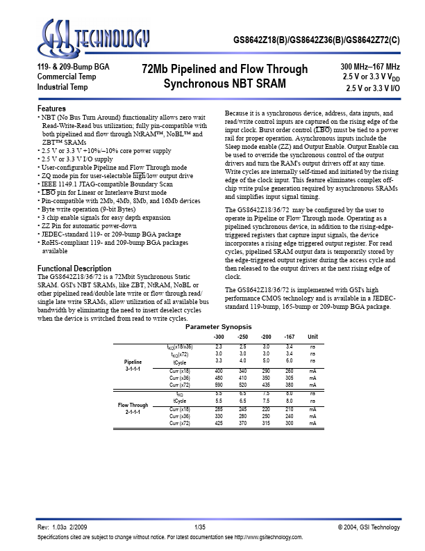
Key Features
- NBT (No Bus Turn Around) functionality allows zero wait Read-Write-Read bus utilization; fully pin-compatible with both pipelined and flow through NtRAM™, NoBL™ and ZBT™ SRAMs
- 2.5 V or 3.3 V +10%/-10% core power supply
- 2.5 V or 3.3 V I/O supply
- User-configurable Pipeline and Flow Through mode
- ZQ mode pin for user-selectable high/low output drive
- IEEE 1149.1 JTAG-compatible Boundary Scan
- LBO pin for Linear or Interleave Burst mode
- Pin-compatible with 2Mb, 4Mb, 8Mb, and 16Mb devices
- Byte write operation (9-bit Bytes)
- 3 chip enable signals for easy depth expansion