Datasheet Summary
Preliminary GS8662Q08/09/18/36E-300/250/200/167 ..
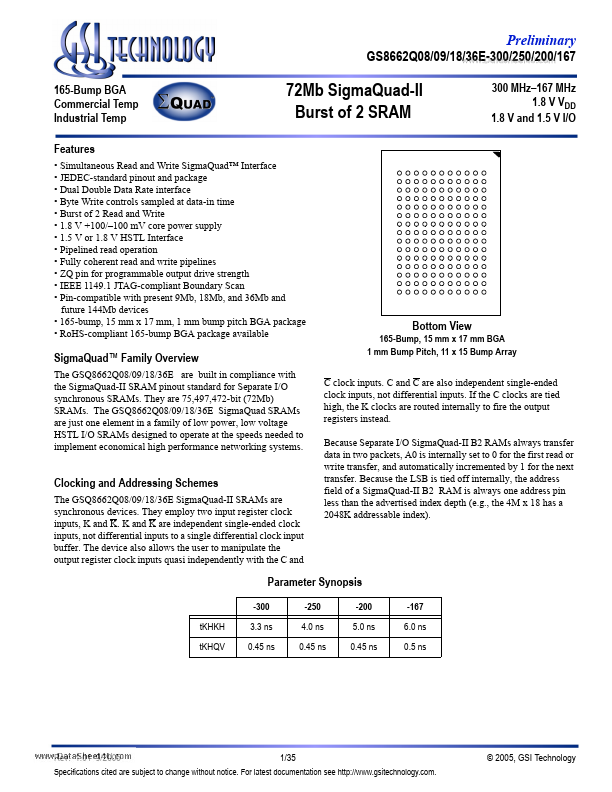
165-Bump BGA mercial Temp Industrial Temp Features
- Simultaneous Read and Write SigmaQuad™ Interface
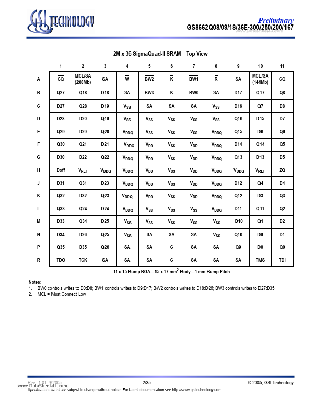
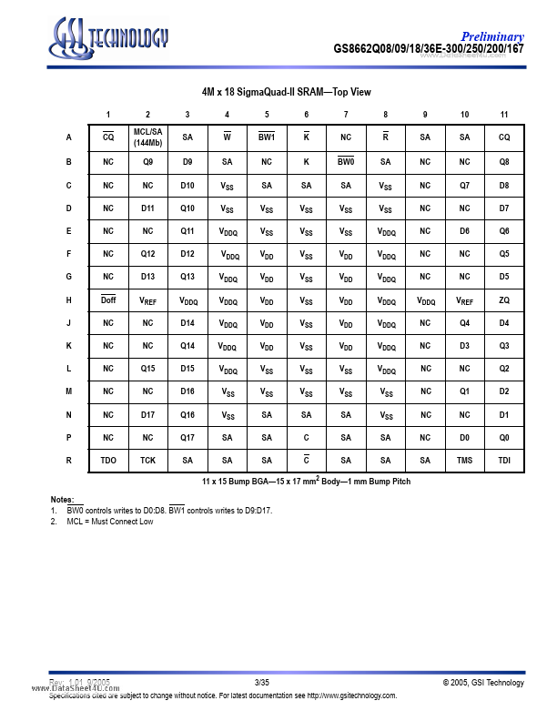
- JEDEC-standard pinout and package
- Dual Double Data Rate interface
- Byte Write controls sampled at data-in time
- Burst of 2 Read and Write
- 1.8 V +100/- 100 mV core power supply
- 1.5 V or 1.8 V HSTL Interface
- Pipelined read operation
- Fully coherent read and write pipelines
- ZQ pin for programmable output drive strength
- IEEE 1149.1 JTAG-pliant Boundary Scan
- Pin-patible with present 9Mb, 18Mb, and 36Mb and future 144Mb devices
- 165-bump, 15 mm x 17 mm, 1 mm bump pitch BGA package
- RoHS-pliant...