Datasheet4U Logo Datasheet4U.com

GS8672D19BGE - 72Mb SigmaQuad-II+ Burst of 4 ECCRAM

Download the GS8672D19BGE datasheet PDF. This datasheet also covers the GS8672D19BE-450 variant, as both devices belong to the same 72mb sigmaquad-ii+ burst of 4 eccram family and are provided as variant models within a single manufacturer datasheet.

General Description

Table Symbol Description Type Comments SA Synchronous Address Inputs Input R Synchronous Read Input Active Low W Synchronous Write Input Active Low BW0 BW3 Synchronous Byte Writes Input Active Low K Input Clock Input Active High K Input Clock Input Active Low

Key Features

  • 2.0 Clock Latency.
  • On-Chip ECC with virtually zero SER.
  • Simultaneous Read and Write SigmaQuad™ Interface.
  • JEDEC-standard pinout and package.
  • Dual Double Data Rate interface.
  • Byte Write Capability due to ECC.
  • Burst of 4 Read and Write.
  • On-Die Termination (ODT) on Data (D), Byte Write (BW), and Clock (K, K) outputs.
  • 1.8 V +100/.
  • 100 mV core power supply.
  • 1.5 V HSTL Interface.
  • Pipelined read o.

📥 Download Datasheet

Note: The manufacturer provides a single datasheet file (GS8672D19BE-450-GSITechnology.pdf) that lists specifications for multiple related part numbers.

Datasheet Details

Part number GS8672D19BGE
Manufacturer GSI Technology
File Size 201.28 KB
Description 72Mb SigmaQuad-II+ Burst of 4 ECCRAM
Datasheet download datasheet GS8672D19BGE Datasheet

Full PDF Text Transcription (Reference)

The following content is an automatically extracted verbatim text from the original manufacturer datasheet and is provided for reference purposes only.

View original datasheet text
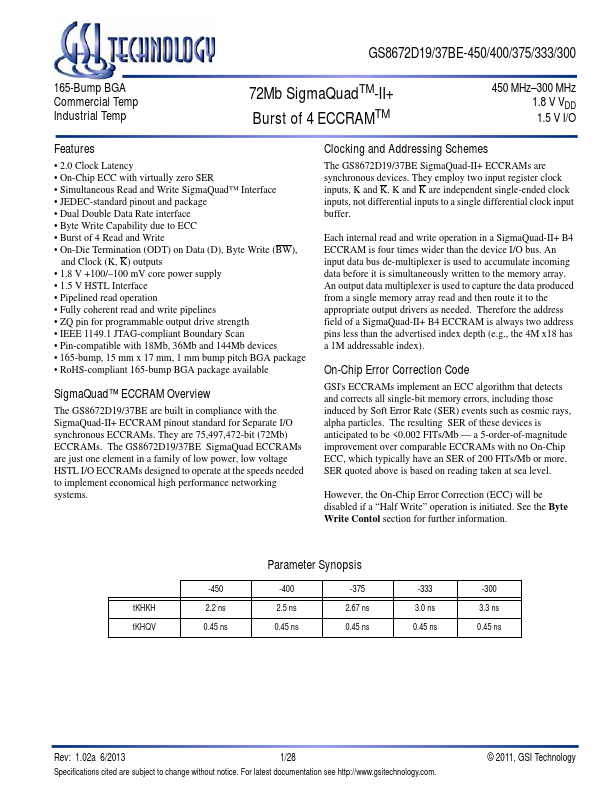
GS8672D19/37BE-450/400/375/333/300 165-Bump BGA Commercial Temp Industrial Temp 72Mb SigmaQuadTM-II+ Burst of 4 ECCRAMTM 450 MHz–300 MHz 1.8 V VDD 1.5 V I/O Features • 2.0 Clock Latency • On-Chip ECC with virtually zero SER • Simultaneous Read and Write SigmaQuad™ Interface • JEDEC-standard pinout and package • Dual Double Data Rate interface • Byte Write Capability due to ECC • Burst of 4 Read and Write • On-Die Termination (ODT) on Data (D), Byte Write (BW), and Clock (K, K) outputs • 1.8 V +100/–100 mV core power supply • 1.5 V HSTL Interface • Pipelined read operation • Fully coherent read and write pipelines • ZQ pin for programmable output drive strength • IEEE 1149.