Datasheet4U Logo Datasheet4U.com

GS8673EQ18BK - 72Mb SigmaQuad-IIIe Burst of 2 ECCRAM

Download the GS8673EQ18BK datasheet PDF. This datasheet also covers the GS8673EQ18BK-675 variant, as both devices belong to the same 72mb sigmaquad-iiie burst of 2 eccram family and are provided as variant models within a single manufacturer datasheet.

Description

Symbol Description SA D[35:0] Q[35:0] QVLD[1:0] CK, CK KD[1:0], KD[1:0] CQ[1:0], CQ[1:0] Address

Read Address is registered on ↑CK and Write Address is registered on ↑CK.

Registered on ↑KD and ↑KD during Write operations.

x18 and x36.

x

Features

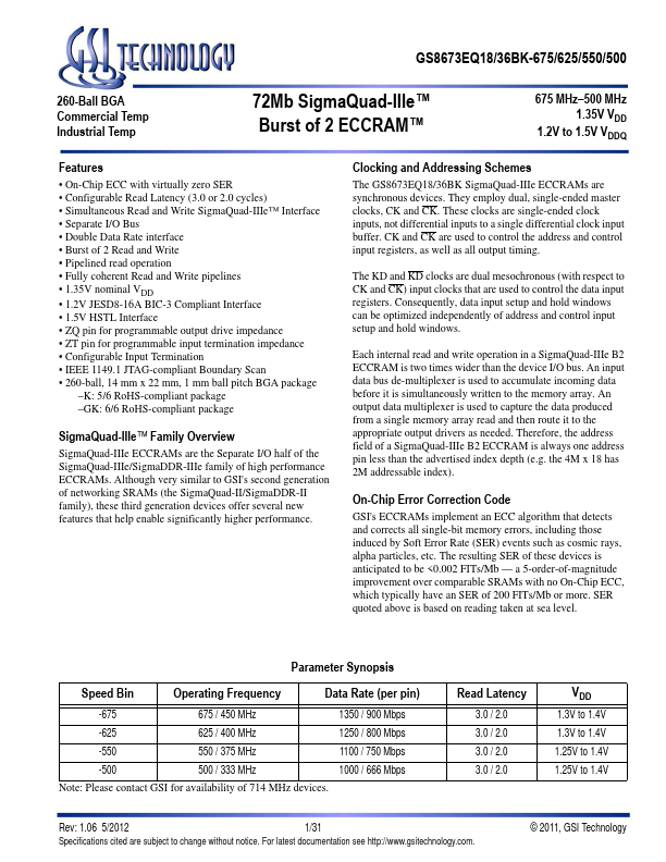
  • On-Chip ECC with virtually zero SER.
  • Configurable Read Latency (3.0 or 2.0 cycles).
  • Simultaneous Read and Write SigmaQuad-IIIe™ Interface.
  • Separate I/O Bus.
  • Double Data Rate interface.
  • Burst of 2 Read and Write.
  • Pipelined read operation.
  • Fully coherent Read and Write pipelines.
  • 1.35V nominal VDD.
  • 1.2V JESD8-16A BIC-3 Compliant Interface.
  • 1.5V HSTL Interface.
  • ZQ pin for programmable output.

📥 Download Datasheet

Note: The manufacturer provides a single datasheet file (GS8673EQ18BK-675-GSITechnology.pdf) that lists specifications for multiple related part numbers.

Datasheet Details

Part number GS8673EQ18BK
Manufacturer GSI Technology
File Size 239.04 KB
Description 72Mb SigmaQuad-IIIe Burst of 2 ECCRAM
Datasheet download datasheet GS8673EQ18BK Datasheet

Full PDF Text Transcription

Click to expand full text
GS8673EQ18/36BK-675/625/550/500 260-Ball BGA Commercial Temp Industrial Temp 72Mb SigmaQuad-IIIe™ Burst of 2 ECCRAM™ 675 MHz–500 MHz 1.35V VDD 1.2V to 1.5V VDDQ Features • On-Chip ECC with virtually zero SER • Configurable Read Latency (3.0 or 2.0 cycles) • Simultaneous Read and Write SigmaQuad-IIIe™ Interface • Separate I/O Bus • Double Data Rate interface • Burst of 2 Read and Write • Pipelined read operation • Fully coherent Read and Write pipelines • 1.35V nominal VDD • 1.2V JESD8-16A BIC-3 Compliant Interface • 1.5V HSTL Interface • ZQ pin for programmable output drive impedance • ZT pin for programmable input termination impedance • Configurable Input Termination • IEEE 1149.
Published: |