Datasheet4U Logo Datasheet4U.com

GS880F18BT-6.5 - 9Mb Sync Burst SRAMs

This page provides the datasheet information for the GS880F18BT-6.5, a member of the GS880F18BT-4.5 9Mb Sync Burst SRAMs family.

Datasheet Summary

Description

Applications The GS880F18/32/36BT is a 9,437,184-bit (8,388,608-bit for x32 version) high performance synchronous SRAM with a 2-bit burst address counter.

Features

  • Flow Through mode operation; Pin 14 = No Connect.
  • 2.5 V or 3.3 V +10%/.
  • 10% core power supply.
  • 2.5 V or 3.3 V I/O supply.
  • LBO pin for Linear or Interleaved Burst mode.
  • Internal input resistors on mode pins allow floating mode pins.
  • Byte Write (BW) and/or Global Write (GW) operation.
  • Internal self-timed write cycle.
  • Automatic power-down for portable.

📥 Download Datasheet

Datasheet preview – GS880F18BT-6.5

Datasheet Details

Part number GS880F18BT-6.5
Manufacturer GSI Technology
File Size 649.27 KB
Description 9Mb Sync Burst SRAMs
Datasheet download datasheet GS880F18BT-6.5 Datasheet
Additional preview pages of the GS880F18BT-6.5 datasheet.
Other Datasheets by GSI Technology

Full PDF Text Transcription

Click to expand full text
GS880F18/32/36BT-4.5/5/5.5/6.5/7.5
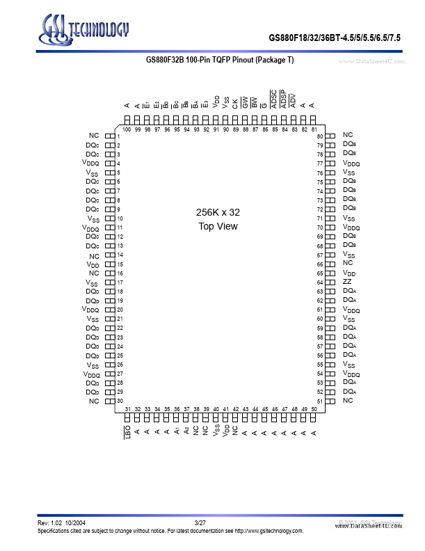
 100-Pin TQFP Commercial Temp Industrial Temp Features • Flow Through mode operation; Pin 14 = No Connect • 2.5 V or 3.3 V +10%/–10% core power supply • 2.5 V or 3.3 V I/O supply • LBO pin for Linear or Interleaved Burst mode • Internal input resistors on mode pins allow floating mode pins • Byte Write (BW) and/or Global Write (GW) operation • Internal self-timed write cycle • Automatic power-down for portable applications • JEDEC-standard 100-lead TQFP package • Pb-Free 100-lead TQFP package available 512K x 18, 256K x 32, 256K x 36 9Mb Sync Burst SRAMs www.DataSheet4U.com 4.5 ns–7.5 ns 2.5 V or 3.3 V VDD 2.5 V or 3.3 V I/O interleave order with the Linear Burst Order (LBO) input. The Burst function need not be used.
Published: |