GS881Z18BD - 9Mb Pipelined and Flow Through Synchronous NBT SRAM
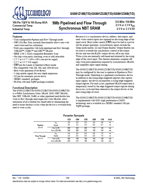
This page provides the datasheet information for the GS881Z18BD, a member of the GS881Z18BT 9Mb Pipelined and Flow Through Synchronous NBT SRAM family.
Datasheet Summary
Description
The GS881Z18B(T/D)/GS881Z32B(T/
Features
User-configurable Pipeline and Flow Through mode.
NBT (No Bus Turn Around) functionality allows zero wait
read-write-read bus utilization.
Fully pin-compatible with both pipelined and flow through
NtRAM™, NoBL™ and ZBT™ SRAMs.
IEEE 1149.1 JTAG-compatible Boundary Scan.
On-chip write parity checking; even or odd selectable.
GS88018AT-133 - 512K x 18/ 256K x 32/ 256K x 36 9Mb Sync Burst SRAMs(ETC)
Other Datasheets by GSI Technology
GS881Z18BD-V- 9Mb Pipelined and Flow Through Synchronous NBT SRAM
GS881Z18BGD- 9Mb Pipelined and Flow Through Synchronous NBT SRAM
GS881Z18BGD-V- 9Mb Pipelined and Flow Through Synchronous NBT SRAM
GS881Z18BGT- 9Mb Pipelined and Flow Through Synchronous NBT SRAM
GS881Z18BGT-V- 9Mb Pipelined and Flow Through Synchronous NBT SRAM
GS881Z18BT- 9Mb Pipelined and Flow Through Synchronous NBT SRAM
GS881Z18BT-V- 9Mb Pipelined and Flow Through Synchronous NBT SRAM
GS881Z18AT- 9Mb Pipelined and Flow Through Synchronous NBT SRAM
Full PDF Text Transcription
Click to expand full text
GS881Z18B(T/D)/GS881Z32B(T/D)/GS881Z36B(T/D)
100-Pin TQFP & 165-Bump BGA 9Mb Pipelined and Flow Through
Commercial Temp Industrial Temp
Synchronous NBT SRAM
333 MHz–150 MHz 2.5 V or 3.3 V VDD 2.5 V or 3.3 V I/O
Features
• User-configurable Pipeline and Flow Through mode • NBT (No Bus Turn Around) functionality allows zero wait
read-write-read bus utilization • Fully pin-compatible with both pipelined and flow through
NtRAM™, NoBL™ and ZBT™ SRAMs • IEEE 1149.1 JTAG-compatible Boundary Scan • On-chip write parity checking; even or odd selectable • 2.5 V or 3.3 V +10%/–10% core power supply • 2.5 V or 3.