G2306A
G2306A is N-CHANNEL ENHANCEMENT MODE POWER MOSFET manufactured by GTM.
..
Pb Free Plating Product
ISSUED DATE :2005/01/17 REVISED DATE :2006/07/17C
N-CHANNEL ENHANCEMENT MODE POWER MOSFET
BVDSS RDS(ON) ID
30V 35m 5A
Description
The G2306A utilized advanced processing techniques to achieve the lowest possible on-resistance, extremely efficient and cost-effectiveness device. The G2306A is universally used for all mercial-industrial applications.
- Capable of 2.5V gate drive
- Lower on-resistance
Features
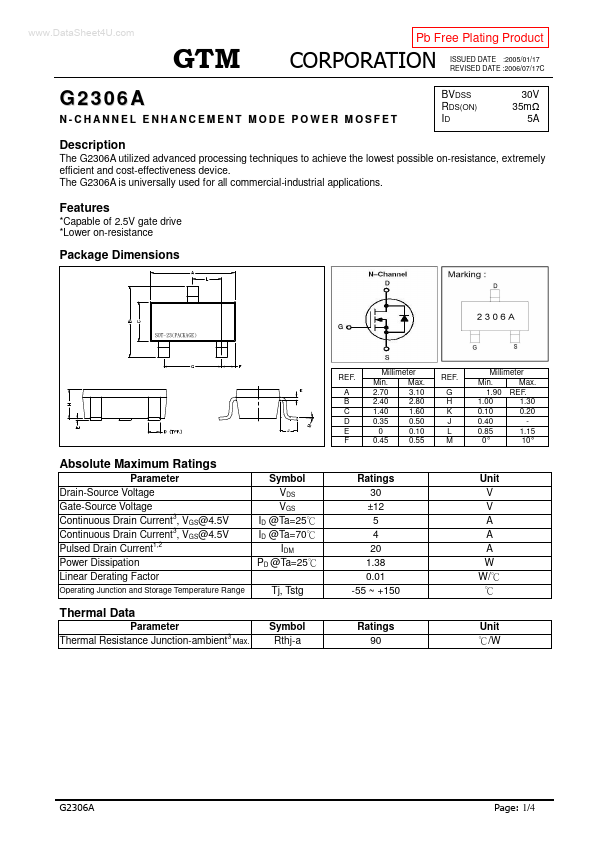
Package Dimensions
REF. A B C D E F
Millimeter Min. Max. 2.70 3.10 2.40 2.80 1.40 1.60 0.35 0.50 0 0.10 0.45 0.55
REF. G H K J L M
Millimeter Min. Max. 1.90 REF. 1.00 1.30 0.10 0.20 0.40 0.85 1.15 0°...