G266
G266 is Complementary Output Hall Effect Latched Sink Driver IC manufactured by GTM.
..
ISSUED DATE :2004/11/03 REVISED DATE :
G266 plementary Output Hall Effect Latched Sink Driver IC
Description
The G266 is an integrated Hall sensors with output drivers designed for electronic mutation of brushless DC motor applications. The device includes an on-chip Hall voltage generator for magnetic sensing, a parator that amplifies the Hall voltage, and a Schmitt trigger to provide switching hysteresis for noise rejection, and plementary open-collector drivers for sinking large current loads. An internal bandgap regulator is used to provide temperature pensated supply voltage for internal circuits and allows a wide operating supply range. If a magnetic flux density larger than threshold Bop, DO is turned on (low) and DOB is turned off (high). The output state is held until a magnetic flux density reversal falls below Brp causing DO to be turned off and DOB turned on. G266 is rated for operation over temperature range from -20 to 100 and voltage range from 3.5V to 28V. The devices are available in low cost die forms or rugged 4 pin SIP packages.
- On-chip Hall sensor IC with two different sensitivity and hysteresis settings for G266
- Internal bandgap regulator allows temperature pensated operations and a wide operating voltage range.
- High output sinking capability up to 300m A for driving large load.
- Lower current change rate reduces the peak output voltages during switching.
- Build in protection diode for chip reverse power connecting.
- Package: SIP-4L.
Features
Application
1)Brushless DC Motor 2)Brushless DC Fan 3)Revolution Counting 4)Speed Measurement
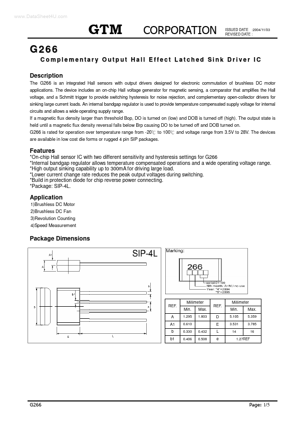
Package Dimensions
REF. A A1 b b1
Millimeter Min.
1.295 0.610 0.330 0.406 0.432 0.508
Max.
REF. D E L e
Millimeter Min.
5.105 3.531 14 1.27REF
Max.
5.359 3.785 16
1/5
ISSUED DATE :2004/11/03 REVISED DATE :
Functional Block Diagrams
VCC 1 2 REG. OUTPUT(DO)
HALL SENSOR 3 OUTPUT(DOB)
Pin Descriptions Name Vcc DO DOB Vss P/I/O P O O P Pin# 1 2 3...