G2N7002 Overview
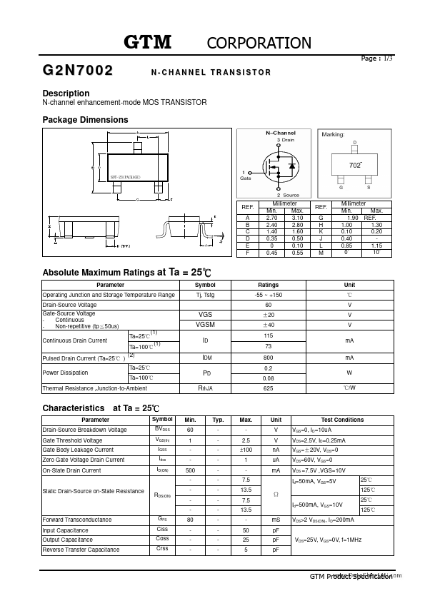
Package Dimensions 1/3 N-CHANNEL TRANSISTOR N-channel enhancement-mode MOS TRANSISTOR REF. A B C D E F Millimeter Min. 2.70 3.10 2.40 2.80 1.40 1.60 0.35 0.50 0 0.10 0.45 0.55 REF.
G2N7002 datasheet by GTM.
| Part number | G2N7002 |
|---|---|
| Datasheet | G2N7002_GTM.pdf |
| File Size | 316.25 KB |
| Manufacturer | GTM |
| Description | N-CHANNELTRANSISTOR |
|
|
Package Dimensions 1/3 N-CHANNEL TRANSISTOR N-channel enhancement-mode MOS TRANSISTOR REF. A B C D E F Millimeter Min. 2.70 3.10 2.40 2.80 1.40 1.60 0.35 0.50 0 0.10 0.45 0.55 REF.
| Part Number | Description |
|---|---|
| G2N7002K | N-CHANNEL ENHANCEMENT MODE POWER MOSFET |
| G2N7000 | N-CHANNEL ENHANCEMENT MODE MOSFET |
| G2N3904 | NPN TRANSISTOR |
| G2N3906 | PNP EPITAXIAL PLANAR TRANSISTOR |
| G2N4401 | NPN EPITAXIAL PLANAR TRANSISTOR |
| G2N4403 | PNP EPITAXIAL PLANAR TRANSISTOR |
| G2N5401 | PNP EPITAXIAL PLANAR TRANSISTOR |
| G2N5551 | NPN EPITAXIAL PLANAR TRANSISTOR |