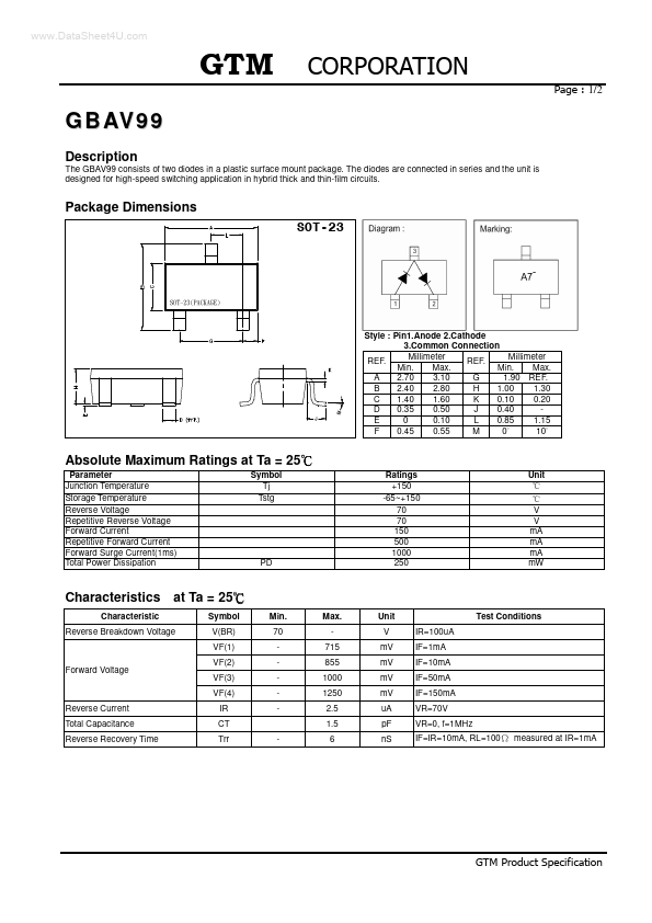
DESCRIPTION
Package Dimensions Style : Pin1.Anode 2.Cathode 3.Common Connection Millimeter Millimeter REF. REF. Min. Max. Min. Max. A 2.70 3.10 G 1.90 REF. B 2.40 2.80 H 1.00 1.30 C 1.40 1.60 K 0.10 0.20 D 0.35 0.50 J 0.40 E 0 0.10 L 0.85 1.15 0 10 F 0.45 0.55 M ABSOLUTE MAXIMUM RATINGS
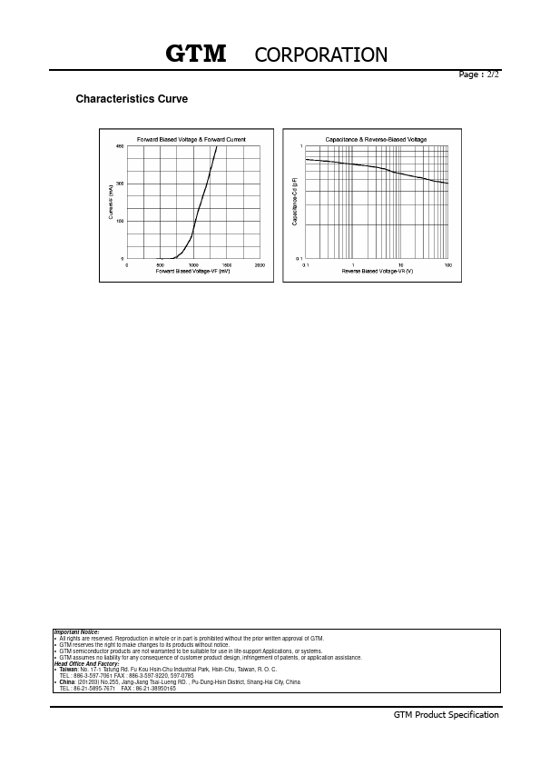
at Ta = 25 Parameter Junction Temperature Storage Temperature Reverse Voltage Repetitive Reverse Voltage Forward Current Repetitive Forward Current Forward Surge Current(1ms) Total Power Dissipation Symbol Tj Tstg Ratings +150 -65~+150 70 70 150 500 1000 250 Unit PD V V mA mA mA mW Characteristics Characteristic at Ta = 25 Symbol V(BR) VF(1) VF(2) VF(3) VF(4) IR CT Trr Min. 70 Max. 715 855 1000 1250 2.5 1.5 6 Unit V mV mV mV mV uA pF nS IR=100uA IF=1mA IF=10mA IF=50mA IF=150mA VR=70V VR=0, f=1MHz IF=IR=10mA, RL=100 measured at IR=1mA Test Conditions Reverse Breakdown Voltage Forward Voltage Reverse Current Total Capacitance Reverse Recovery Time 2/2 Characteristics Curve Important Notice: All rights are reserved. GTM