Datasheet Summary
..
Pb Free Plating Product
ISSUED DATE :2005/03/03 REVISED DATE :
Description
N-CHANNEL ENHANCEMENT MODE POWER MOSFET
BVDSS RDS(ON) ID
18V 25m 35A
The GI9916 provide the designer with the best bination of fast switching, ruggedized device design, ultra low on-resistance and cost-effectiveness.
- Single Drive Requirement
- Low on-resistance
- Capable of 2.5V gate drive
- Low drive current
Features
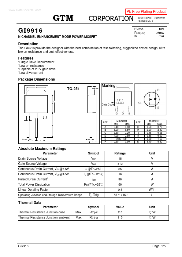
Package Dimensions TO-251
REF. A B C D E F
Millimeter Min. Max. 6.40 6.80 5.20 5.50 6.80 7.20 7.20 7.80 2.30 REF. 0.60 0.90
REF. G H J K L M
Millimeter Min. Max. 0.50 0.70 2.20 2.40 0.45 0.55 0.45 0.60 0.90 1.50 5.40...