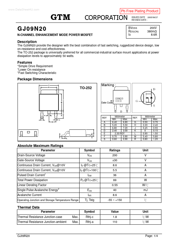
GJ09N20 Overview
The GJ09N20 provide the designer with the best bination of fast switching, ruggedized device design, low on-resistance and cost-effectiveness. The TO-252 package is universally preferred for all mercial-industrial surface mount applications at power dissipation levels to approximately 50 watts.
GJ09N20 Key Features
- Simple Drive Requirement -Lower On-resistance -Fast Switching Characteristic