GJ9960
GJ9960 is N-CHANNEL ENHANCEMENT MODE POWER MOSFET manufactured by GTM.
Description
The GJ9960 provides the designer with the best bination of fast switching, ruggedized device design, low on-resistance and cost-effectiveness.
Features
- Simple Drive Requirement
- Low Gate Charge
- Fast Switching
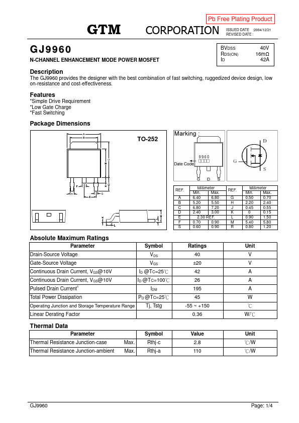
Package Dimensions
TO-252
REF.
A B C D E F S
Millimeter
Min.
Max.
2.30 REF.
REF.
G H J K L M R
Millimeter
Min. Max.
0.50 0.70
2.20 2.40
0.45 0.55
0.90 1.50
5.40 5.80
0.80 1.20
Absolute Maximum Ratings
Parameter...